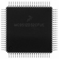
MC9S12D32CFUE Freescale Semiconductor, MC9S12D32CFUE Datasheet - Page 56

MC9S12D32CFUE
Manufacturer Part Number
MC9S12D32CFUE
Description
IC MCU 32K FLASH 25MHZ 80-QFP
Manufacturer
Freescale Semiconductor
Series
HCS12r
Specifications of MC9S12D32CFUE
Core Processor
HCS12
Core Size
16-Bit
Speed
25MHz
Connectivity
CAN, I²C, SCI, SPI
Peripherals
PWM, WDT
Number Of I /o
59
Program Memory Size
32KB (32K x 8)
Program Memory Type
FLASH
Eeprom Size
1K x 8
Ram Size
4K x 8
Voltage - Supply (vcc/vdd)
2.35 V ~ 5.25 V
Data Converters
A/D 8x10b
Oscillator Type
Internal
Operating Temperature
-40°C ~ 85°C
Package / Case
80-QFP
Processor Series
S12D
Core
HCS12
Data Bus Width
16 bit
Data Ram Size
4 KB
Interface Type
CAN/I2C/SCI/SPI
Maximum Clock Frequency
25 MHz
Number Of Programmable I/os
49
Number Of Timers
8
Maximum Operating Temperature
+ 85 C
Mounting Style
SMD/SMT
3rd Party Development Tools
EWHCS12
Development Tools By Supplier
M68KIT912DP256
Minimum Operating Temperature
- 40 C
On-chip Adc
2 (8-ch x 10-bit)
Lead Free Status / RoHS Status
Lead free / RoHS Compliant
Available stocks
Company
Part Number
Manufacturer
Quantity
Price
Company:
Part Number:
MC9S12D32CFUE
Manufacturer:
Freescale Semiconductor
Quantity:
10 000
MC9S12DJ64 Device User Guide — V01.20
2.3 Detailed Signal Descriptions
2.3.1 EXTAL, XTAL — Oscillator Pins
EXTAL and XTAL are the crystal driver and external clock pins. On reset all the device clocks are derived
from the EXTAL input frequency. XTAL is the crystal output.
2.3.2 RESET — External Reset Pin
An active low bidirectional control signal, it acts as an input to initialize the MCU to a known start-up
state, and an output when an internal MCU function causes a reset.
2.3.3 TEST — Test Pin
This input only pin is reserved for test.
NOTE:
The TEST pin must be tied to VSS in all applications.
2.3.4 VREGEN — Voltage Regulator Enable Pin
This input only pin enables or disables the on-chip voltage regulator.
2.3.5 XFC — PLL Loop Filter Pin
PLL loop filter. Please ask your Freescale representative for the interactive application note to compute
PLL loop filter elements. Any current leakage on this pin must be avoided.
XFC
R
0
C
P
MCU
C
S
VDDPLL
VDDPLL
Figure 2-3 PLL Loop Filter Connections
2.3.6 BKGD / TAGHI / MODC — Background Debug, Tag High, and Mode Pin
The BKGD/TAGHI/MODC pin is used as a pseudo-open-drain pin for the background debug
communication. In MCU expanded modes of operation when instruction tagging is on, an input low on
this pin during the falling edge of E-clock tags the high half of the instruction word being read into the
56


