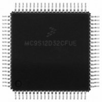
MC9S12D32CFUE Freescale Semiconductor, MC9S12D32CFUE Datasheet - Page 78

MC9S12D32CFUE
Manufacturer Part Number
MC9S12D32CFUE
Description
IC MCU 32K FLASH 25MHZ 80-QFP
Manufacturer
Freescale Semiconductor
Series
HCS12r
Specifications of MC9S12D32CFUE
Core Processor
HCS12
Core Size
16-Bit
Speed
25MHz
Connectivity
CAN, I²C, SCI, SPI
Peripherals
PWM, WDT
Number Of I /o
59
Program Memory Size
32KB (32K x 8)
Program Memory Type
FLASH
Eeprom Size
1K x 8
Ram Size
4K x 8
Voltage - Supply (vcc/vdd)
2.35 V ~ 5.25 V
Data Converters
A/D 8x10b
Oscillator Type
Internal
Operating Temperature
-40°C ~ 85°C
Package / Case
80-QFP
Processor Series
S12D
Core
HCS12
Data Bus Width
16 bit
Data Ram Size
4 KB
Interface Type
CAN/I2C/SCI/SPI
Maximum Clock Frequency
25 MHz
Number Of Programmable I/os
49
Number Of Timers
8
Maximum Operating Temperature
+ 85 C
Mounting Style
SMD/SMT
3rd Party Development Tools
EWHCS12
Development Tools By Supplier
M68KIT912DP256
Minimum Operating Temperature
- 40 C
On-chip Adc
2 (8-ch x 10-bit)
Lead Free Status / RoHS Status
Lead free / RoHS Compliant
Available stocks
Company
Part Number
Manufacturer
Quantity
Price
Company:
Part Number:
MC9S12D32CFUE
Manufacturer:
Freescale Semiconductor
Quantity:
10 000
MC9S12DJ64 Device User Guide — V01.20
6.4 HCS12 Interrupt (INT) Block Description
Consult the INT Block Guide for information on the HCS12 Interrupt module.
6.5 HCS12 Background Debug (BDM) Block Description
Consult the BDM Block Guide for information on the HCS12 Background Debug module.
6.5.1 Device-specific information
When the BDM Block Guide refers to alternate clock this is equivalent to Oscillator Clock.
6.6 HCS12 Breakpoint (BKP) Block Description
Consult the BKP Block Guide for information on the HCS12 Breakpoint module.
Section 7 Clock and Reset Generator (CRG) Block
Description
Consult the CRG Block User Guide for information about the Clock and Reset Generator module.
7.1 Device-specific information
The Low Voltage Reset feature of the CRG is not available on this device.
Section 8 Oscillator (OSC) Block Description
Consult the OSC Block User Guide for information about the Oscillator module.
8.1 Device-specific information
The XCLKS input signal is active low (see 2.3.13 PE7 / NOACC / XCLKS — Port E I/O Pin 7).
Section 9 Enhanced Capture Timer (ECT) Block
Description
Consult the ECT_16B8C Block User Guide for information about the Enhanced Capture Timer module.
When the ECT_16B8C Block User Guide refers to freeze mode this is equivalent to active BDM mode.
78


