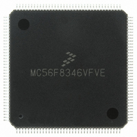
MC56F8346VFVE Freescale Semiconductor, MC56F8346VFVE Datasheet - Page 117

MC56F8346VFVE
Manufacturer Part Number
MC56F8346VFVE
Description
IC DSP 16BIT 60MHZ 144-LQFP
Manufacturer
Freescale Semiconductor
Series
56F8xxxr
Datasheet
1.MC56F8346VFVE.pdf
(178 pages)
Specifications of MC56F8346VFVE
Core Processor
56800
Core Size
16-Bit
Speed
60MHz
Connectivity
CAN, EBI/EMI, SCI, SPI
Peripherals
POR, PWM, Temp Sensor, WDT
Number Of I /o
62
Program Memory Size
136KB (68K x 16)
Program Memory Type
FLASH
Ram Size
6K x 16
Voltage - Supply (vcc/vdd)
2.25 V ~ 3.6 V
Data Converters
A/D 16x12b
Oscillator Type
External
Operating Temperature
-40°C ~ 105°C
Package / Case
144-LQFP
Product
DSPs
Data Bus Width
16 bit
Processor Series
MC56F83xx
Core
56800E
Numeric And Arithmetic Format
Fixed-Point
Device Million Instructions Per Second
60 MIPs
Maximum Clock Frequency
60 MHz
Number Of Programmable I/os
62
Data Ram Size
4 KB
Operating Supply Voltage
3 V to 3.6 V
Maximum Operating Temperature
+ 105 C
Mounting Style
SMD/SMT
Interface Type
SCI, SPI
Minimum Operating Temperature
- 40 C
On-chip Adc
12 bit, 4 Channel
Package
144LQFP
Family Name
56F8xxx
Maximum Speed
60 MHz
Number Of Timers
16
For Use With
MC56F8367EVME - EVAL BOARD FOR MC56F83X
Lead Free Status / RoHS Status
Lead free / RoHS Compliant
Eeprom Size
-
Lead Free Status / Rohs Status
Lead free / RoHS Compliant
Available stocks
Company
Part Number
Manufacturer
Quantity
Price
Company:
Part Number:
MC56F8346VFVE
Manufacturer:
Freescale
Quantity:
3
Company:
Part Number:
MC56F8346VFVE
Manufacturer:
FREESCAL
Quantity:
275
Company:
Part Number:
MC56F8346VFVE
Manufacturer:
Freescale Semiconductor
Quantity:
10 000
Part Number:
MC56F8346VFVE
Manufacturer:
FREESCALE
Quantity:
20 000
6.5.6.8
This bit controls the pull-up resistors on the FAULTB0, FAULTB1, FAULTB2, and FAULTB3 pins.
6.5.6.9
This bit controls the pull-up resistors on the FAULTA0, FAULTA1, and FAULTA2 pins.
6.5.6.10
This bit field is reserved or not implemented. It is read as 0 and cannot be modified by writing.
6.5.6.11
This bit controls the pull-up resistors on the WR and RD pins.
6.5.6.12
This bit field is reserved or not implemented. It is read as 0 and cannot be modified by writing.
6.5.6.13
This bit controls the pull-up resistors on the TRST, TMS and TDI pins.
6.5.6.14
This bit field is reserved or not implemented. It is read as 0 and cannot be modified by writing.
6.5.7
The CLKO select register can be used to multiplex out any one of the clocks generated inside the clock
generation and SIM modules. The default value is SYS_CLK. All other clocks primarily muxed out are
for test purposes only, and are subject to significant unspecified latencies at high frequencies.
The upper four bits of the GPIOB register can function as GPIO, A[23:20], or as additional clock output
signals. GPIO has priority and is enabled/disabled via the GPIOB_PER. If GPIOB[7:4] are programmed
to operate as peripheral outputs, then the choice between A[23:20] and additional clock outputs is done
here in the CLKOSR. The default state is for the peripheral function of GPIOB[7:4] to be programmed as
A[23:20]. This can be changed by altering A[23:20], as shown in
6.5.7.1
This bit field is reserved or not implemented. It is read as 0 and cannot be modified by writing.
Freescale Semiconductor
Preliminary
Base + $A
RESET
Read
Write
CLKO Select Register (SIM_CLKOSR)
PWMB—Bit 8
PWMA0—Bit 7
Reserved—Bit 6
CTRL—Bit 5
Reserved—Bit 4
JTAG—Bit 3
Reserved—Bits 2 - 0
Reserved—Bits 15–10
15
0
0
14
0
0
Figure 6-9 CLKO Select Register (SIM_CLKOSR)
13
0
0
12
0
0
56F8346 Technical Data, Rev. 15
11
0
0
10
0
0
A23
9
0
A22
8
0
A21
7
0
Figure
A20
6
0
CLK
DIS
5
1
6-9.
4
0
3
0
CLKOSEL
2
0
Register Descriptions
1
0
0
0
117


