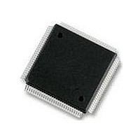
MCF53010CQT240 Freescale Semiconductor, MCF53010CQT240 Datasheet - Page 43

MCF53010CQT240
Manufacturer Part Number
MCF53010CQT240
Description
MCU 32BIT COLDFIRE EMAC 208LQFP
Manufacturer
Freescale Semiconductor
Series
MCF5301xr
Datasheet
1.MCF53010CQT240.pdf
(62 pages)
Specifications of MCF53010CQT240
Core Processor
Coldfire V3
Core Size
32-Bit
Speed
240MHz
Connectivity
EBI/EMI, Ethernet, I²C, MMC, SPI, SSI, UART/USART, USB OTG
Peripherals
DMA, PWM, WDT
Number Of I /o
61
Program Memory Size
16KB (16K x 8)
Program Memory Type
Cache
Ram Size
128K x 8
Voltage - Supply (vcc/vdd)
1.08 V ~ 3.6 V
Oscillator Type
Internal
Operating Temperature
-40°C ~ 85°C
Package / Case
208-LQFP
Processor Series
MCF5301x
Core
ColdFire V3
Data Bus Width
32 bit
Data Ram Size
128 KB
Interface Type
UART, I2C, SPI, SSI, Ethernet
Maximum Clock Frequency
20 MHz to 400 MHz
Number Of Programmable I/os
61
Number Of Timers
8
Operating Supply Voltage
3.6 V
Maximum Operating Temperature
+ 85 C
Mounting Style
SMD/SMT
3rd Party Development Tools
JLINK-CF-BDM26, EWCF
Development Tools By Supplier
M53015EVB, M53017KIT, M53017MOD
Minimum Operating Temperature
- 40 C
Lead Free Status / RoHS Status
Lead free / RoHS Compliant
Eeprom Size
-
Data Converters
-
Lead Free Status / Rohs Status
Lead free / RoHS Compliant
5.17
Each SIM card interface consist of a total of 12 pins (two separate ports of six pins each. Mostly one port with 5 pins is used).
The interface is meant to be used with synchronous SIM cards. This means that the SIM module provides a clock for the SIM
card to use. The frequency of this clock is normally 372 times the data rate on the TX/RX pins, however SIM module can work
with CLK equal to 16 times the data rate on TX/RX pins.
There is no timing relationship between the clock and the data. The clock that the SIM module provides to the SIM card is used
by the SIM card to recover the clock from the data, like a standard UART. All six (or five when a bidirectional TXRX is used)
of the pins for each half of the SIM module are asynchronous to each other. There are no required timing relationships between
the signals in normal mode. However, there are some in reset and power down sequences.
5.17.1
Figure 30
Freescale Semiconductor
Bus Signal Line Load
Open Drain Signal Level
Bus Signal Levels
Num
10
11
12
13
14
5
6
7
8
9
shows the timing of the SIM module, and
SIM Electrical Specifications
Power Up Time
Supply Current
Pull-up Resistance
Open Drain Resistance
Output High Voltage
Output Low Voltage
Output HIGH Voltage
Output LOW Voltage
Input HIGH Voltage
Input LOW Voltage
SIM_CLK
General Timing Requirements
Parameter
Table 28. MMC/SD Interface Electrical Specifications (continued)
Preliminary—Subject to Change Without Notice
Figure 30. SIM Clock Timing Diagram
Design
Value
Sfall
NA
MCF5301x Data Sheet, Rev. 5
47
—
—
—
—
—
—
—
—
Table 29
0.625 x V
0.75 x V
V
V
DD
SS
Min
100
NA
10
—
—
—
– 0.3
lists the timing parameters.
– 0.2
DD
DD
1/Sfreq
0.125 x V
0.25 x V
V
Srise
DD
Max
250
200
100
NA
0.3
—
—
+ 3
DD
DD
kohm Internal PU
kohm For MMC cards only
Unit
Preliminary Electrical Characteristics
mA
ms
V
V
V
V
V
V
For MMC cards only
I
I
I
I
OH
OL
OH
OL
= 2 mA
= 100 µA @V
= –100 µA
= –100 µA @V
Condition/Remark
DD
DD
min
min
43


