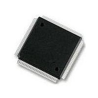
MCF53012CQT240 Freescale Semiconductor, MCF53012CQT240 Datasheet - Page 25

MCF53012CQT240
Manufacturer Part Number
MCF53012CQT240
Description
MCU 32BIT COLDFIRE EMAC 208LQFP
Manufacturer
Freescale Semiconductor
Series
MCF5301xr
Datasheet
1.MCF53010CQT240.pdf
(62 pages)
Specifications of MCF53012CQT240
Core Processor
Coldfire V3
Core Size
32-Bit
Speed
240MHz
Connectivity
EBI/EMI, Ethernet, I²C, MMC, SPI, SSI, UART/USART, USB OTG
Peripherals
DMA, PWM, WDT
Number Of I /o
61
Program Memory Size
16KB (16K x 8)
Program Memory Type
Cache
Ram Size
128K x 8
Voltage - Supply (vcc/vdd)
1.08 V ~ 3.6 V
Oscillator Type
Internal
Operating Temperature
-40°C ~ 85°C
Package / Case
208-LQFP
Processor Series
MCF5301x
Core
ColdFire V3
Data Bus Width
32 bit
Data Ram Size
128 KB
Interface Type
UART, I2C, SPI, SSI, Ethernet
Maximum Clock Frequency
20 MHz to 400 MHz
Number Of Programmable I/os
61
Number Of Timers
8
Operating Supply Voltage
3.6 V
Maximum Operating Temperature
+ 85 C
Mounting Style
SMD/SMT
3rd Party Development Tools
JLINK-CF-BDM26, EWCF
Development Tools By Supplier
M53015EVB, M53017KIT, M53017MOD
Minimum Operating Temperature
- 40 C
Lead Free Status / RoHS Status
Lead free / RoHS Compliant
Eeprom Size
-
Data Converters
-
Lead Free Status / Rohs Status
Lead free / RoHS Compliant
5.6
Table 12
5.6.1
A multi-function external bus interface called FlexBus is provided with basic functionality to interface to slave-only devices up
to a maximum bus frequency of 80MHz. It can be directly connected to asynchronous or synchronous devices such as external
boot ROMs, flash memories, gate-array logic, or other simple target (slave) devices with little or no additional circuitry. For
asynchronous devices a simple chip-select based interface can be used. The FlexBus interface has six general purpose
chip-selects (FB_CS[5:0]) which can be configured to be distributed between the FlexBus or SDRAM memory interfaces.
Freescale Semiconductor
8
9
10
11
Jitter is the average deviation from the programmed frequency measured over the specified interval at maximum f
Measurements are made with the device powered by filtered supplies and clocked by a stable external clock signal.
Noise injected into the PLL circuitry via PLL V
the Cjitter percentage for a given interval.
Values are with frequency modulation disabled. If frequency modulation is enabled, jitter is the sum of Cjitter+Cmod.
Modulation percentage applies over an interval of 10μs, or equivalently the modulation rate is 100kHz.
Modulation range determined by hardware design.
* The timings are also valid for inputs sampled on the negative clock edge.
lists processor bus input timings.
External Interface Timing Characteristics
FlexBus
FB_CLK
All processor bus timings are synchronous; that is, input setup/hold and output delay with
respect to the rising edge of a reference clock. The reference clock is the FB_CLK output.
All other timing relationships can be derived from these values. Timings listed in
are shown in
Inputs
Input Setup And Hold
FB_CLK (80MHz)
Figure 11
Input Rise Time
Input Fall Time
Figure 10. General Input Timing Requirements
Preliminary—Subject to Change Without Notice
B4
and
Figure
MCF5301x Data Sheet, Rev. 5
DD
12.
, EV
Invalid
DD
NOTE
, and V
V
V
V
V
h
h
l
l
= V
= V
= V
= V
IH
IH
TSETUP
IL
IL
1.5V
SS
and variation in crystal oscillator frequency increase
Valid
1.5V
THOLD
1.5V
t
t
rise
fall
Preliminary Electrical Characteristics
Invalid
B5
Table 12
sys
.
25


