MC9S12DG256CFUE Freescale Semiconductor, MC9S12DG256CFUE Datasheet - Page 58
MC9S12DG256CFUE
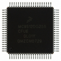
Manufacturer Part Number
MC9S12DG256CFUE
Description
IC MCU 256K FLASH 4K EE 80-QFP
Manufacturer
Freescale Semiconductor
Series
HCS12r
Specifications of MC9S12DG256CFUE
Core Processor
HCS12
Core Size
16-Bit
Speed
25MHz
Connectivity
CAN, I²C, SCI, SPI
Peripherals
PWM, WDT
Number Of I /o
59
Program Memory Size
256KB (256K x 8)
Program Memory Type
FLASH
Eeprom Size
4K x 8
Ram Size
12K x 8
Voltage - Supply (vcc/vdd)
2.35 V ~ 5.25 V
Data Converters
A/D 16x10b
Oscillator Type
Internal
Operating Temperature
-40°C ~ 85°C
Package / Case
80-QFP
Processor Series
S12D
Core
HCS12
Data Bus Width
16 bit
Data Ram Size
12 KB
Interface Type
CAN/I2C/SCI/SPI
Maximum Clock Frequency
25 MHz
Number Of Programmable I/os
91
Number Of Timers
1
Operating Supply Voltage
- 0.3 V to + 6 V
Maximum Operating Temperature
+ 85 C
Mounting Style
SMD/SMT
3rd Party Development Tools
EWHCS12
Development Tools By Supplier
M68KIT912DP256
Minimum Operating Temperature
- 40 C
On-chip Adc
2 (8-ch x 10-bit)
Package
80PQFP
Family Name
HCS12
Maximum Speed
25 MHz
Lead Free Status / RoHS Status
Lead free / RoHS Compliant
Available stocks
Company
Part Number
Manufacturer
Quantity
Price
Company:

Part Number:
MC9S12DG256CFUE
Manufacturer:
freescaie
Quantity:
6
Company:
Part Number:
MC9S12DG256CFUE
Manufacturer:
Freescale Semiconductor
Quantity:
10 000
Part Number:
MC9S12DG256CFUE
Manufacturer:
FREESCALE
Quantity:
20 000


Freescale Semiconductor, Inc.
MC9S12DT128B Device User Guide — V01.09
2.3.6 PAD[15] / AN1[7] / ETRIG1 — Port AD Input Pin [15]
PAD15 is a general purpose input pin and analog input of the analog to digital converter ATD1. It can act
as an external trigger input for the ATD1.
2.3.7 PAD[14:8] / AN1[6:0] — Port AD Input Pins [14:8]
PAD14 - PAD8 are general purpose input pins and analog inputs of the analog to digital converter ATD1.
2.3.8 PAD[7] / AN0[7] / ETRIG0 — Port AD Input Pin [7]
PAD7 is a general purpose input pin and analog input of the analog to digital converter ATD0. It can act
as an external trigger input for the ATD0.
2.3.9 PAD[6:0] / AN0[6:0] — Port AD Input Pins [6:0]
PAD6 - PAD8 are general purpose input pins and analog inputs of the analog to digital converter ATD0.
2.3.10 PA[7:0] / ADDR[15:8] / DATA[15:8] — Port A I/O Pins
PA7-PA0 are general purpose input or output pins. In MCU expanded modes of operation, these pins are
used for the multiplexed external address and data bus.
2.3.11 PB[7:0] / ADDR[7:0] / DATA[7:0] — Port B I/O Pins
PB7-PB0 are general purpose input or output pins. In MCU expanded modes of operation, these pins are
used for the multiplexed external address and data bus.
2.3.12 PE7 / NOACC / XCLKS — Port E I/O Pin 7
PE7 is a general purpose input or output pin. During MCU expanded modes of operation, the NOACC
signal, when enabled, is used to indicate that the current bus cycle is an unused or “free” cycle. This signal
will assert when the CPU is not using the bus.
The XCLKS is an input signal which controls whether a crystal in combination with the internal Colpitts
(low power) oscillator is used or whether Pierce oscillator/external clock circuitry is used. The state of this
pin is latched at the rising edge of RESET. If the input is a logic low the EXTAL pin is configured for an
external clock drive. If input is a logic high an oscillator circuit is configured on EXTAL and XTAL. Since
this pin is an input with a pull-up device during reset, if the pin is left floating, the default configuration is
an oscillator circuit on EXTAL and XTAL.
For More Information On This Product,
Go to: www.freescale.com
Related parts for MC9S12DG256CFUE
Image
Part Number
Description
Manufacturer
Datasheet
Request
R

Part Number:
Description:
Manufacturer:
Freescale Semiconductor, Inc
Datasheet:
Part Number:
Description:
Manufacturer:
Freescale Semiconductor, Inc
Datasheet:
Part Number:
Description:
Manufacturer:
Freescale Semiconductor, Inc
Datasheet:
Part Number:
Description:
Manufacturer:
Freescale Semiconductor, Inc
Datasheet:
Part Number:
Description:
Manufacturer:
Freescale Semiconductor, Inc
Datasheet:
Part Number:
Description:
Manufacturer:
Freescale Semiconductor, Inc
Datasheet:
Part Number:
Description:
Manufacturer:
Freescale Semiconductor, Inc
Datasheet:
Part Number:
Description:
Manufacturer:
Freescale Semiconductor, Inc
Datasheet:
Part Number:
Description:
Manufacturer:
Freescale Semiconductor, Inc
Datasheet:
Part Number:
Description:
Manufacturer:
Freescale Semiconductor, Inc
Datasheet:
Part Number:
Description:
Manufacturer:
Freescale Semiconductor, Inc
Datasheet:
Part Number:
Description:
Manufacturer:
Freescale Semiconductor, Inc
Datasheet:
Part Number:
Description:
Manufacturer:
Freescale Semiconductor, Inc
Datasheet:
Part Number:
Description:
Manufacturer:
Freescale Semiconductor, Inc
Datasheet:
Part Number:
Description:
Manufacturer:
Freescale Semiconductor, Inc
Datasheet: