MC9S12DG256CFUE Freescale Semiconductor, MC9S12DG256CFUE Datasheet - Page 65
MC9S12DG256CFUE
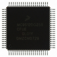
Manufacturer Part Number
MC9S12DG256CFUE
Description
IC MCU 256K FLASH 4K EE 80-QFP
Manufacturer
Freescale Semiconductor
Series
HCS12r
Specifications of MC9S12DG256CFUE
Core Processor
HCS12
Core Size
16-Bit
Speed
25MHz
Connectivity
CAN, I²C, SCI, SPI
Peripherals
PWM, WDT
Number Of I /o
59
Program Memory Size
256KB (256K x 8)
Program Memory Type
FLASH
Eeprom Size
4K x 8
Ram Size
12K x 8
Voltage - Supply (vcc/vdd)
2.35 V ~ 5.25 V
Data Converters
A/D 16x10b
Oscillator Type
Internal
Operating Temperature
-40°C ~ 85°C
Package / Case
80-QFP
Processor Series
S12D
Core
HCS12
Data Bus Width
16 bit
Data Ram Size
12 KB
Interface Type
CAN/I2C/SCI/SPI
Maximum Clock Frequency
25 MHz
Number Of Programmable I/os
91
Number Of Timers
1
Operating Supply Voltage
- 0.3 V to + 6 V
Maximum Operating Temperature
+ 85 C
Mounting Style
SMD/SMT
3rd Party Development Tools
EWHCS12
Development Tools By Supplier
M68KIT912DP256
Minimum Operating Temperature
- 40 C
On-chip Adc
2 (8-ch x 10-bit)
Package
80PQFP
Family Name
HCS12
Maximum Speed
25 MHz
Lead Free Status / RoHS Status
Lead free / RoHS Compliant
Available stocks
Company
Part Number
Manufacturer
Quantity
Price
Company:

Part Number:
MC9S12DG256CFUE
Manufacturer:
freescaie
Quantity:
6
Company:
Part Number:
MC9S12DG256CFUE
Manufacturer:
Freescale Semiconductor
Quantity:
10 000
Part Number:
MC9S12DG256CFUE
Manufacturer:
FREESCALE
Quantity:
20 000


2.3.51 PS5 / MOSI0 — Port S I/O Pin 5
PS5 is a general purpose input or output pin. It can be configured as master output (during master mode)
or slave input pin (during slave mode) MOSI of the Serial Peripheral Interface 0 (SPI0).
2.3.52 PS4 / MISO0 — Port S I/O Pin 4
PS4 is a general purpose input or output pin. It can be configured as master input (during master mode) or
slave output pin (during slave mode) MOSI of the Serial Peripheral Interface 0 (SPI0).
2.3.53 PS3 / TXD1 — Port S I/O Pin 3
PS3 is a general purpose input or output pin. It can be configured as the transmit pin TXD of Serial
Communication Interface 1 (SCI1).
2.3.54 PS2 / RXD1 — Port S I/O Pin 2
PS2 is a general purpose input or output pin. It can be configured as the receive pin RXD of Serial
Communication Interface 1 (SCI1).
2.3.55 PS1 / TXD0 — Port S I/O Pin 1
PS1 is a general purpose input or output pin. It can be configured as the transmit pin TXD of Serial
Communication Interface 0 (SCI0).
2.3.56 PS0 / RXD0 — Port S I/O Pin 0
PS0 is a general purpose input or output pin. It can be configured as the receive pin RXD of Serial
Communication Interface 0 (SCI0).
2.3.57 PT[7:0] / IOC[7:0] — Port T I/O Pins [7:0]
PT7-PT0 are general purpose input or output pins. They can be configured as input capture or output
compare pins IOC7-IOC0 of the Enhanced Capture Timer (ECT).
2.4 Power Supply Pins
MC9S12DT128B power and ground pins are described below.
Mnemonic
VDD1, 2
VSS1, 2
Table 2-2 MC9S12DT128B Power and Ground Connection Summary
112-pin QFP
Pin Number
13, 65
14, 66
Freescale Semiconductor, Inc.
Nominal
Voltage
For More Information On This Product,
2.5V
0V
Go to: www.freescale.com
Internal power and ground generated by internal regulator
MC9S12DT128B Device User Guide — V01.09
Description
Related parts for MC9S12DG256CFUE
Image
Part Number
Description
Manufacturer
Datasheet
Request
R

Part Number:
Description:
Manufacturer:
Freescale Semiconductor, Inc
Datasheet:
Part Number:
Description:
Manufacturer:
Freescale Semiconductor, Inc
Datasheet:
Part Number:
Description:
Manufacturer:
Freescale Semiconductor, Inc
Datasheet:
Part Number:
Description:
Manufacturer:
Freescale Semiconductor, Inc
Datasheet:
Part Number:
Description:
Manufacturer:
Freescale Semiconductor, Inc
Datasheet:
Part Number:
Description:
Manufacturer:
Freescale Semiconductor, Inc
Datasheet:
Part Number:
Description:
Manufacturer:
Freescale Semiconductor, Inc
Datasheet:
Part Number:
Description:
Manufacturer:
Freescale Semiconductor, Inc
Datasheet:
Part Number:
Description:
Manufacturer:
Freescale Semiconductor, Inc
Datasheet:
Part Number:
Description:
Manufacturer:
Freescale Semiconductor, Inc
Datasheet:
Part Number:
Description:
Manufacturer:
Freescale Semiconductor, Inc
Datasheet:
Part Number:
Description:
Manufacturer:
Freescale Semiconductor, Inc
Datasheet:
Part Number:
Description:
Manufacturer:
Freescale Semiconductor, Inc
Datasheet:
Part Number:
Description:
Manufacturer:
Freescale Semiconductor, Inc
Datasheet:
Part Number:
Description:
Manufacturer:
Freescale Semiconductor, Inc
Datasheet: