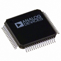
ADUC7128BSTZ126-RL Analog Devices Inc, ADUC7128BSTZ126-RL Datasheet - Page 19

ADUC7128BSTZ126-RL
Manufacturer Part Number
ADUC7128BSTZ126-RL
Description
IC DAS MCU ARM7 ADC/DDS 64-LQFP
Manufacturer
Analog Devices Inc
Series
MicroConverter® ADuC7xxxr
Datasheet
1.EVAL-ADUC7128QSPZ.pdf
(92 pages)
Specifications of ADUC7128BSTZ126-RL
Core Size
16/32-Bit
Program Memory Size
126KB (126K x 8)
Core Processor
ARM7
Speed
41.78MHz
Connectivity
I²C, SPI, UART/USART
Peripherals
PLA, POR, PWM, PSM, Temp Sensor, WDT
Number Of I /o
28
Program Memory Type
FLASH
Ram Size
8K x 8
Voltage - Supply (vcc/vdd)
3 V ~ 3.6 V
Data Converters
A/D 10x12b; D/A 1x10b
Oscillator Type
Internal
Operating Temperature
-40°C ~ 125°C
Package / Case
64-LQFP
Controller Family/series
(ARM7) ADUC
No. Of I/o's
40
Cpu Speed
41.78MHz
No. Of Timers
5
Digital Ic Case Style
LQFP
Embedded Interface Type
I2C, SPI, UART
Rohs Compliant
Yes
Lead Free Status / RoHS Status
Lead free / RoHS Compliant
For Use With
EVAL-ADUC7128QSPZ - KIT DEV FOR ADUC7128
Eeprom Size
-
Lead Free Status / RoHS Status
Lead free / RoHS Compliant, Lead free / RoHS Compliant
Other names
ADUC7128BSTZ126-RLTR
Available stocks
Company
Part Number
Manufacturer
Quantity
Price
Company:
Part Number:
ADUC7128BSTZ126-RL
Manufacturer:
Analog Devices Inc
Quantity:
10 000
Pin
No.
17
18
19
20
21
22
23, 53, 67
24, 54
25
26
27
28
29
30
31
32
33
34
35
36
37
38
39
40
41
42
43
44
45
46
47
48
49
50
51
52
55
56
57
58
59
60
61
62
Mnemonic
P4.6/SPM10/AD14
P4.7/SPM11/AD15
P0.0/BM/CMP
P0.6/T1/MRST
TCK
TDO/P0.2/BHE
IOGND
IOV
LV
DGND
P3.0/PWM1/AD0
P3.1/PWM2/AD1
P3.2/PWM3/AD2
P3.3/PWM4/AD3
P2.4/MS0
P0.3/ADC
P2.5/MS1
P2.6/MS2
RST
P3.4/PWM5/AD4
P3.5/PWM6/AD5
P0.4/IRQ0/CONVST/MS1
P0.5/IRQ1/ADC
P2.0/SPM9
P0.7/SPM8/ECLK/XCLK
XCLKO
XCLKI
PV
DGND
P3.6/AD6
P3.7/AD7
P2.7/MS3
P2.1/WS
P2.2/RS
P1.7/SPM7
P1.6/SPM6
P4.0/S1/AD8
P4.1/S2/AD9
P1.5/SPM5
P1.4/SPM4
P1.3/SPM3
P1.2/SPM2
P1.1/SPM1
P1.0/SPM0
DD
DD
DD
BUSY
/TRST/A16
OUT
BUSY
/MS0
Type
I/O
I/O
I/O
O
I
O
S
S
S
S
I/O
I/O
I/O
I/O
I/O
I/O
I/O
I/O
I
I/O
I/O
I/O
I/O
I/O
I/O
O
I
S
S
I/O
I/O
I/O
I/O
I/O
I/O
I/O
I/O
I/O
I/O
I/O
I/O
I/O
I/O
I/O
1
Description
General-Purpose Input and Output Port 4.6/Serial Port Mux Pin 10/External Memory AD14.
General-Purpose Input and Output Port 4.7/Serial Port Mux Pin 11/External Memory AD15.
General-Purpose Input and Output Port 0.0 /Boot Mode. The ADuC7129 enters download
mode if BM is low at reset and executes code if BM is pulled high at reset through a 1 kΩ
resistor/voltage comparator output/external memory MS0.
General-Purpose Output Port 0.6/Timer1 Input/Power-On Reset Output/External Memory AE.
JTAG Test Port Input, Test Clock. Debug and download access.
JTAG Test Port Output, Test Data Out. Debug and download access/general-purpose input
and output Port 0.2/External Memory BHE.
Ground for GPIO. Typically connected to DGND.
3.3 V Supply for GPIO and Input of the On-Chip Voltage Regulator.
2.5 V Output of the On-Chip Voltage Regulator. Must be connected to a 0.47 μF capacitor
to DGND.
Ground for Core Logic.
General-Purpose Input and Output Port 3.0/PWM1 Output/External Memory AD0.
General-Purpose Input and Output Port 3.1/PWM2 Output/External Memory AD1.
General-Purpose Input and Output Port 3.2/PWM3 Output/External Memory AD2.
General-Purpose Input and Output Port 3.3/PWM4 Output//External Memory AD3.
General-Purpose Input and Output Port 2.4/Memory Select 0.
General-Purpose Input and Output Port 3.3/ADC
Debug and download access/External Memory A16.
General-Purpose Input and Output Port 2.5/Memory Select 1.
General-Purpose Input and Output Port 2.6/Memory Select 2.
Reset Input (Active Low).
General-Purpose Input and Output Port 3.4/PWM5 Output/External Memory AD4.
General-Purpose Input and Output Port 3.5/PWM6 Output/External Memory AD5.
General-Purpose Input and Output Port 0.5/External Interrupt Request 0, Active High/Start
Conversion Input Signal for ADC/External Memory MS1.
General-Purpose Input and Output Port 0.6/External Interrupt Request 1, Active
High/ADC
General-Purpose Input and Output Port 2.0/Serial Port Mux Pin 9.
General-Purpose Input and Output Port 0.7/Serial Port Mux Pin 8/Output for the External
Clock Signal/Input to the Internal Clock Generator Circuits.
Output from the Crystal Oscillator Inverter.
Input to the Crystal Oscillator Inverter and Input to the Internal Clock Generator Circuits.
2.5 V PLL Supply. Must be connected to a 0.1 μF capacitor to DGND. Should be connected
to 2.5 V LDO output.
Ground for PLL.
General-Purpose Input and Output Port 3.6/External Memory AD6.
General-Purpose Input and Output Port 3.7/External Memory AD7.
General-Purpose Input and Output Port 2.7/Memory Select 3.
General-Purpose Input and Output Port 2.1/Memory Write Select.
General-Purpose Input and Output Port 2.1/Memory Read Select.
General-Purpose Input and Output Port 1.7/Serial Port Mux Pin 7.
General-Purpose Input and Output Port 1.6/Serial Port Mux Pin 6.
General-Purpose Input and Output Port 4.0/Quadrature Input 1/External Memory AD8.
General-Purpose Input and Output Port 4.1/Quadrature Input 2/External Memory AD9.
General-Purpose Input and Output Port 1.5/Serial Port Mux Pin 5.
General-Purpose Input and Output Port 1.4/Serial Port Mux Pin 4.
General-Purpose Input and Output Port 1.3/Serial Port Mux Pin 3.
General-Purpose Input and Output Port 1.2/Serial Port Mux Pin 2.
General-Purpose Input and Output Port 1.1/Serial Port Mux Pin 1.
General-Purpose Input and Output Port 1.0/Serial Port Mux Pin 0.
Rev. 0 | Page 19 of 92
BUSY
Signal.
BUSY
Signal/JTAG Test Port Input, Test Reset.
ADuC7128/ADuC7129


