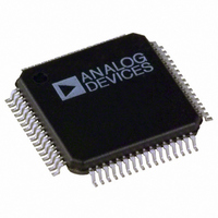
ADUC7128BSTZ126-RL Analog Devices Inc, ADUC7128BSTZ126-RL Datasheet - Page 45

ADUC7128BSTZ126-RL
Manufacturer Part Number
ADUC7128BSTZ126-RL
Description
IC DAS MCU ARM7 ADC/DDS 64-LQFP
Manufacturer
Analog Devices Inc
Series
MicroConverter® ADuC7xxxr
Datasheet
1.EVAL-ADUC7128QSPZ.pdf
(92 pages)
Specifications of ADUC7128BSTZ126-RL
Core Size
16/32-Bit
Program Memory Size
126KB (126K x 8)
Core Processor
ARM7
Speed
41.78MHz
Connectivity
I²C, SPI, UART/USART
Peripherals
PLA, POR, PWM, PSM, Temp Sensor, WDT
Number Of I /o
28
Program Memory Type
FLASH
Ram Size
8K x 8
Voltage - Supply (vcc/vdd)
3 V ~ 3.6 V
Data Converters
A/D 10x12b; D/A 1x10b
Oscillator Type
Internal
Operating Temperature
-40°C ~ 125°C
Package / Case
64-LQFP
Controller Family/series
(ARM7) ADUC
No. Of I/o's
40
Cpu Speed
41.78MHz
No. Of Timers
5
Digital Ic Case Style
LQFP
Embedded Interface Type
I2C, SPI, UART
Rohs Compliant
Yes
Lead Free Status / RoHS Status
Lead free / RoHS Compliant
For Use With
EVAL-ADUC7128QSPZ - KIT DEV FOR ADUC7128
Eeprom Size
-
Lead Free Status / RoHS Status
Lead free / RoHS Compliant, Lead free / RoHS Compliant
Other names
ADUC7128BSTZ126-RLTR
Available stocks
Company
Part Number
Manufacturer
Quantity
Price
Company:
Part Number:
ADUC7128BSTZ126-RL
Manufacturer:
Analog Devices Inc
Quantity:
10 000
OTHER ANALOG PERIPHERALS
DAC
The ADuC7128/ADuC7129 feature a 10-bit current DAC that
can be used to generate user-defined waveforms or sine waves
generated by the DDS. The DAC consists of a 10-bit IDAC
followed by a current-to-voltage conversion.
The current output of the IDAC is passed through a resistor and
capacitor network where it is both filtered and converted to a
voltage. This voltage is then buffered by an op amp and passed
to the line driver.
Table 49. DACCON MMR Bit Designations
Bit
10:9
8
7
6
5
4
3
2:1
0
Value
00
01
10
11
Description
Reserved. These bits should be written to 0 by the user.
Reserved. This bit should be written to 0 by the user.
Reserved. This bit should be written to 0 by the user.
Reserved. This bit should be written to 0 by the user.
Output Enable. This bit operates in all modes. In Line Driver mode, this bit should be set.
Single-Ended or Differential Output Control.
Reserved. This bit should be set to 0 by the user.
Operation Mode Control. This bit selects the mode of operation of the DAC.
Power-Down.
Reserved.
Reserved.
DDS and DAC Mode. Selected by DACEN.
DAC Update Rate Control. This bit has no effect when in DDS mode.
Set by user to enable the line driver output.
Cleared by user to disable the line driver output. In this mode the line driver output is high impedance.
Set by user to operate in differential mode, the output is the differential voltage between LD1TX and LD2TX. The voltage
output range is V
Cleared by user to reference the LD1TX output to AGND. The voltage output range is AV
Set by user to update the DAC on the negative edge of Timer1. This allows the user to use any one of the core CLK, OSC
CLK, baud CLK, or user CLK and divide these down by 1, 16, 256, or 32,768. A user can do waveform generation by
writing to the DAC data register from RAM and updating the DAC at regular intervals via Timer1.
Cleared by user to update the DAC on the negative edge of HCLK.
REF
/2 ± V
REF
/2.
Rev. 0 | Page 45 of 92
For the DAC to function, the internal 2.5 V voltage reference
must be enabled and driven out onto an external capacitor,
REFCON = 0x01.
Once the DAC is enabled, users see a 5 mV drop in the internal
reference value. This is due to bias currents drawn from the
reference used in the DAC circuitry. It is recommended that if
using the DAC, it be left powered on to avoid seeing variations
in ADC results.
ADuC7128/ADuC7129
DD
/2 ± V
REF
/2.


