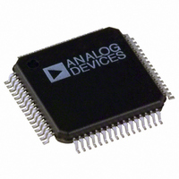
ADUC7128BSTZ126-RL Analog Devices Inc, ADUC7128BSTZ126-RL Datasheet - Page 88

ADUC7128BSTZ126-RL
Manufacturer Part Number
ADUC7128BSTZ126-RL
Description
IC DAS MCU ARM7 ADC/DDS 64-LQFP
Manufacturer
Analog Devices Inc
Series
MicroConverter® ADuC7xxxr
Datasheet
1.EVAL-ADUC7128QSPZ.pdf
(92 pages)
Specifications of ADUC7128BSTZ126-RL
Core Size
16/32-Bit
Program Memory Size
126KB (126K x 8)
Core Processor
ARM7
Speed
41.78MHz
Connectivity
I²C, SPI, UART/USART
Peripherals
PLA, POR, PWM, PSM, Temp Sensor, WDT
Number Of I /o
28
Program Memory Type
FLASH
Ram Size
8K x 8
Voltage - Supply (vcc/vdd)
3 V ~ 3.6 V
Data Converters
A/D 10x12b; D/A 1x10b
Oscillator Type
Internal
Operating Temperature
-40°C ~ 125°C
Package / Case
64-LQFP
Controller Family/series
(ARM7) ADUC
No. Of I/o's
40
Cpu Speed
41.78MHz
No. Of Timers
5
Digital Ic Case Style
LQFP
Embedded Interface Type
I2C, SPI, UART
Rohs Compliant
Yes
Lead Free Status / RoHS Status
Lead free / RoHS Compliant
For Use With
EVAL-ADUC7128QSPZ - KIT DEV FOR ADUC7128
Eeprom Size
-
Lead Free Status / RoHS Status
Lead free / RoHS Compliant, Lead free / RoHS Compliant
Other names
ADUC7128BSTZ126-RLTR
Available stocks
Company
Part Number
Manufacturer
Quantity
Price
Company:
Part Number:
ADUC7128BSTZ126-RL
Manufacturer:
Analog Devices Inc
Quantity:
10 000
ADuC7128/ADuC7129
In these cases, tie the AGND pins and IOGND pins of the
ADuC7128/ADuC7129 to the analog ground plane, as shown
in Figure 69b. In systems with only one ground plane, ensure
that the digital and analog components are physically separated
onto separate halves of the board such that digital return currents
do not flow near analog circuitry and vice versa. The ADuC7128/
ADuC7129 can then be placed between the digital and analog
sections, as illustrated in Figure 69c.
In all of these scenarios, and in more complicated real-life
applications, keep in mind the flow of current from the supplies
and back to ground. Make sure the return paths for all currents
are as close as possible to the paths the currents took to reach
their destinations. For example, do not power components on
the analog side (see Figure 69b) with IOV
force return currents from IOV
Avoid digital currents from flowing under analog circuitry,
which could happen if the user places a noisy digital chip on the
left half of the board (see Figure 69c). Whenever possible, avoid
large discontinuities in the ground planes (such as are formed
by a long trace on the same layer) because they force return
signals to travel a longer path. Make all connections to the ground
plane directly, with little or no trace separating the pin from its
via to ground.
b.
a.
c.
PLACE ANALOG
COMPONENTS
COMPONENTS HERE
COMPONENTS HERE
PLACE ANALOG
PLACE ANALOG
HERE
Figure 69. System Grounding Schemes
AGND
AGND
GND
DD
to flow through AGND.
COMPONENTS HERE
COMPONENTS HERE
COMPONENTS HERE
PLACE DIGITAL
PLACE DIGITAL
PLACE DIGITAL
DD
DGND
DGND
since that would
Rev. 0 | Page 88 of 92
If a user plans to connect fast logic signals (rise/fall time < 5 ns)
to any of the digital inputs of the ADuC7128/ADuC7129, add
a series resistor to each relevant line to keep rise and fall times
longer than 5 ns at the ADuC7128/ADuC7129 input pins.
A value of 100 Ω or 200 Ω is usually sufficient to prevent high
speed signals from coupling capacitively into the ADuC7128/
ADuC7129 and affecting the accuracy of ADC conversions.
CLOCK OSCILLATOR
The clock source for the ADuC7128/ADuC7129 can be gener-
ated by the internal PLL or by an external clock input. To use
the internal PLL, connect a 32.768 kHz parallel resonant crystal
between XCLKI and XCLKO as shown Figure 70. External
capacitors should be connected as per the crystal manufacturer’s
recommendations. Note that the crystal pads already have an
internal capacitance of typically 10 pF. Users should ensure that
the total capacitance (10 pF internal + external capacitance)
does not exceed the manufacturer rating.
The 32 kHz crystal allows the PLL to lock correctly to give a
frequency of 41.78 MHz. If no external crystal is present, the
internal oscillator is used to give a frequency of 41.78 MHz ±
3% typically.
To use an external source clock input instead of the PLL, Bit 1
and Bit 0 of PLLCON must be modified. The external clock
uses the XCLK pin.
Whether using the internal PLL or an external clock source, the
specified operational clock speed range of the ADuC7128/
ADuC7129 is 50 kHz to 41.78 MHz to ensure correct operation
of the analog peripherals and Flash/EE.
Figure 70. External Parallel Resonant Crystal Connections
12pF
12pF
Figure 71. Connecting an External Clock Source
EXTERNAL
SOURCE
CLOCK
32.768kHz
XCLKO
XCLKI
XCLKI
XCLK
ADuC7128
ADuC7128
TO
FREQUENCY
DIVIDER
TO
INTERNAL
PLL


