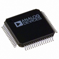
ADUC7128BSTZ126-RL Analog Devices Inc, ADUC7128BSTZ126-RL Datasheet - Page 33

ADUC7128BSTZ126-RL
Manufacturer Part Number
ADUC7128BSTZ126-RL
Description
IC DAS MCU ARM7 ADC/DDS 64-LQFP
Manufacturer
Analog Devices Inc
Series
MicroConverter® ADuC7xxxr
Datasheet
1.EVAL-ADUC7128QSPZ.pdf
(92 pages)
Specifications of ADUC7128BSTZ126-RL
Core Size
16/32-Bit
Program Memory Size
126KB (126K x 8)
Core Processor
ARM7
Speed
41.78MHz
Connectivity
I²C, SPI, UART/USART
Peripherals
PLA, POR, PWM, PSM, Temp Sensor, WDT
Number Of I /o
28
Program Memory Type
FLASH
Ram Size
8K x 8
Voltage - Supply (vcc/vdd)
3 V ~ 3.6 V
Data Converters
A/D 10x12b; D/A 1x10b
Oscillator Type
Internal
Operating Temperature
-40°C ~ 125°C
Package / Case
64-LQFP
Controller Family/series
(ARM7) ADUC
No. Of I/o's
40
Cpu Speed
41.78MHz
No. Of Timers
5
Digital Ic Case Style
LQFP
Embedded Interface Type
I2C, SPI, UART
Rohs Compliant
Yes
Lead Free Status / RoHS Status
Lead free / RoHS Compliant
For Use With
EVAL-ADUC7128QSPZ - KIT DEV FOR ADUC7128
Eeprom Size
-
Lead Free Status / RoHS Status
Lead free / RoHS Compliant, Lead free / RoHS Compliant
Other names
ADUC7128BSTZ126-RLTR
Available stocks
Company
Part Number
Manufacturer
Quantity
Price
Company:
Part Number:
ADUC7128BSTZ126-RL
Manufacturer:
Analog Devices Inc
Quantity:
10 000
TYPICAL OPERATION
Once configured via the ADC control and channel selection
registers, the ADC converts the analog input and provides
an 11-bit result in the ADC data register.
The top four bits are the sign bits, and the 12-bit result is placed
from Bit 16 to Bit 27, as shown in Figure 35. For fully differential
mode, the result is ±11 bits. Again, it should be noted that in
fully differential mode, the result is represented in twos comple-
ment format shifted one bit to the right, and in pseudo differential
and single-ended mode, the result is represented in straight
binary format.
ADC MMRs Interface
The ADC is controlled and configured via a number of MMRs (see Table 32) that are described in detail in the following pages.
Table 32. ADC MMRs
Name
ADCCON
ADCCP
ADCCN
ADCSTA
ADCDAT
ADCRST
31
SIGN BITS
SIGN
BIT
0 1111 1111 1110
0 1111 1111 1100
0 1111 1111 1010
0 0000 0000 0001
0 0000 0000 0000
1 1111 1111 1110
1 0000 0000 0100
1 0000 0000 0010
1 0000 0000 0000
Figure 34. ADC Transfer Function in Differential Mode
Description
ADC Control Register. Allows the programmer to enable the ADC peripheral, to select the mode of operation of the ADC (either
single-ended, pseudo differential, or fully differential mode), and to select the conversion type (see Table 33).
ADC Positive Channel Selection Register.
ADC Negative Channel Selection Register.
ADC Status Register. Indicates when an ADC conversion result is ready. The ADCSTA register contains only one bit, ADCREADY
(Bit 0), representing the status of the ADC. This bit is set at the end of an ADC conversion generating an ADC interrupt. It is
cleared automatically by reading the ADCDAT MMR. When the ADC is performing a conversion, the status of the ADC can be
read externally via the ADC
This information can be available on P0.5 (see the General-Purpose I/O section) if enabled in the GP0CON register.
ADC Data Result Register. Holds the 12-bit ADC result, as shown in Table 35.
ADC Reset Register. Resets all the ADC registers to their default values.
27
–V
Figure 35. ADC Result Format
REF
1LSB =
+ 1LSB
12-BIT ADC RESULT
2 × V
VOLTAGE INPUT (V
4096
REF
0LSB
Busy
pin. This pin is high during a conversion. When the conversion is finished, ADC
IN
+ – V
16 15
IN
+V
–)
REF
– 1LSB
0
Rev. 0 | Page 33 of 92
Current Consumption
The ADC in standby mode, that is, powered up but not
converting, typically consumes 640 μA. The internal reference
adds 140 μA. During conversion, the extra current is 0.3 μA,
multiplied by the sampling frequency (in kHz).
Timing
Figure 36 gives details of the ADC timing. Users control the
ADC clock speed and the number of acquisition clock in the
ADCCON MMR. By default, the acquisition time is eight clocks
and the clock divider is two. The number of extra clocks (such
as bit trial or write) is set to 19, giving a sampling rate of 774 kSPS.
For conversion on the temperature sensor, the ADC acquisition
time is automatically set to 16 clocks and the ADC clock divider
is set to 32. When using multiple channels, including the
temperature sensor, the timing settings revert back to the user-
defined settings after reading the temperature sensor channel.
ADC CLOCK
CONV
ADC
ADCDAT
START
BUSY
Figure 36. ADC Timing
ACQ
ADuC7128/ADuC7129
BIT TRIAL
ADCSTA = 0
WRITE
ADC INTERRUPT
DATA
Busy
goes back low.
ADCSTA = 1


