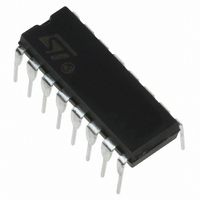
ST7FLITES5Y0B6 STMicroelectronics, ST7FLITES5Y0B6 Datasheet - Page 113

ST7FLITES5Y0B6
Manufacturer Part Number
ST7FLITES5Y0B6
Description
MCU 8BIT 1K FLASH 16DIP
Manufacturer
STMicroelectronics
Series
ST7r
Datasheet
1.ST7FLITES2Y0B6.pdf
(124 pages)
Specifications of ST7FLITES5Y0B6
Core Processor
ST7
Core Size
8-Bit
Speed
8MHz
Connectivity
SPI
Peripherals
LVD, POR, PWM, WDT
Number Of I /o
13
Program Memory Size
1KB (1K x 8)
Program Memory Type
FLASH
Ram Size
128 x 8
Voltage - Supply (vcc/vdd)
2.4 V ~ 5.5 V
Data Converters
A/D 5x10b
Oscillator Type
Internal
Operating Temperature
-40°C ~ 85°C
Package / Case
16-DIP (0.300", 7.62mm)
Processor Series
ST7FLITESx
Core
ST7
Data Bus Width
8 bit
Data Ram Size
128 B
Interface Type
SPI
Maximum Clock Frequency
8 MHz
Number Of Programmable I/os
13
Number Of Timers
2
Operating Supply Voltage
2.4 V to 5.5 V
Maximum Operating Temperature
+ 85 C
Mounting Style
Through Hole
Development Tools By Supplier
ST7FLIT0-IND/USB, ST7FLITE-SK/RAIS, ST7MDT10-DVP3, ST7MDT10-EMU3, STX-RLINK
Minimum Operating Temperature
- 40 C
On-chip Adc
8 bit
For Use With
497-5858 - EVAL BOARD PLAYBACK ST7FLITE497-5049 - KIT STARTER RAISONANCE ST7FLITE
Lead Free Status / RoHS Status
Lead free / RoHS Compliant
Eeprom Size
-
Lead Free Status / Rohs Status
Details
Other names
497-4862
Available stocks
Company
Part Number
Manufacturer
Quantity
Price
OPTION BYTES (Cont’d)
OPTION BYTE 1
Bit 7 = PLLx4x8 PLL Factor selection.
0: PLLx4
1: PLLx8
Bit 6 = PLLOFF PLL disabled
0: PLL enabled
1: PLL disabled (by-passed)
Bit 5 = Reserved, must always be 1.
Table 21. List of valid option combinations
Note: see Clock Management Block diagram in
Bits 3:2 = LVD[1:0] Low voltage detection selec-
tion
These option bits enable the LVD block with a se-
lected threshold as shown in
Table 22. LVD Threshold Configuration
Default
V
2.4V - 3.3V
3.3V - 5.5V
LVD Off
Highest Voltage Threshold (∼4.1V)
Medium Voltage Threshold (∼3.5V)
Lowest Voltage Threshold (∼2.8V)
Value
DD
range
7
1
Operating conditions
Configuration
Reserved
Clock Source
Internal RC 1%
External clock
Internal RC 1%
External clock
1
1
OPTION BYTE 0
1
Table
SEC1 SEC0
1
22.
LVD1 LVD0
1
1
1
0
0
PLL
off
x4
x8
off
x4
x8
off
x4
x8
off
x4
x8
FMP
R
0
1
0
1
0
Figure 14
FMP
W
0
0
Bit 4 = OSC RC Oscillator selection
0: RC oscillator on
1: RC oscillator off
Note: If the RC oscillator is selected, then to im-
prove clock stability and frequency accuracy, it is
recommended to place a decoupling capacitor,
typically 100nF, between the V
close as possible to the ST7 device.
Bit 1 = WDG SW Hardware or software watchdog
This option bit selects the watchdog type.
0: Hardware (watchdog always enabled)
1: Software (watchdog to be enabled by software)
Bit 0 = WDG HALT Watchdog Reset on Halt
This option bit determines if a RESET is generated
when entering HALT mode while the Watchdog is
active.
0: No Reset generation when entering Halt mode
1: Reset generation when entering Halt mode
Typ f
0.7MHz @3V
2.8MHz @3V
-
0-4MHz
4MHz
-
1MHz @5V
-
8MHz @5V
0-8MHz
-
8 MHz
x4x8
PLL
7
1
CPU
OFF
PLL
1
1
ST7LITE0xY0, ST7LITESxY0
OPTION BYTE 1
OSC
OSC LVD1 LVD0
0
0
1
1
0
0
1
1
-
-
-
-
0
Option Bits
1
PLLOFF
DD
1
0
1
0
1
0
1
0
-
-
-
-
1
and V
WDG
SW
SS
1
PLLx4x8
pins as
113/124
1
0
1
0
1
1
1
1
HALT
-
-
-
-
WDG
0
1


