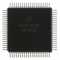
MC9S12C32MFUE25 Freescale Semiconductor, MC9S12C32MFUE25 Datasheet - Page 188

MC9S12C32MFUE25
Manufacturer Part Number
MC9S12C32MFUE25
Description
IC MCU 32K FLASH 25MHZ 80-QFP
Manufacturer
Freescale Semiconductor
Series
HCS12r
Datasheets
1.MC9S12GC16MFUE.pdf
(690 pages)
2.MC9S12C96CFUER.pdf
(26 pages)
3.MC9S12C32CFAE25.pdf
(2 pages)
Specifications of MC9S12C32MFUE25
Core Processor
HCS12
Core Size
16-Bit
Speed
25MHz
Connectivity
CAN, EBI/EMI, SCI, SPI
Peripherals
POR, PWM, WDT
Number Of I /o
60
Program Memory Size
32KB (32K x 8)
Program Memory Type
FLASH
Ram Size
2K x 8
Voltage - Supply (vcc/vdd)
2.35 V ~ 5.5 V
Data Converters
A/D 8x10b
Oscillator Type
Internal
Operating Temperature
-40°C ~ 125°C
Package / Case
80-QFP
Processor Series
S12C
Core
HCS12
Data Bus Width
16 bit
Data Ram Size
2 KB
Interface Type
CAN/SCI/SPI
Maximum Clock Frequency
25 MHz
Number Of Programmable I/os
60
Number Of Timers
8
Operating Supply Voltage
3.3 V to 5.5 V
Maximum Operating Temperature
+ 125 C
Mounting Style
SMD/SMT
3rd Party Development Tools
EWHCS12
Development Tools By Supplier
M68EVB912C32EE
Minimum Operating Temperature
- 40 C
On-chip Adc
8-ch x 10-bit
For Use With
CML12C32SLK - KIT STUDENT LEARNING 16BIT HCS12
Lead Free Status / RoHS Status
Lead free / RoHS Compliant
Eeprom Size
-
Lead Free Status / Rohs Status
Lead free / RoHS Compliant
Available stocks
Company
Part Number
Manufacturer
Quantity
Price
Company:
Part Number:
MC9S12C32MFUE25
Manufacturer:
Freescale Semiconductor
Quantity:
10 000
Part Number:
MC9S12C32MFUE25
Manufacturer:
FREESCALE
Quantity:
20 000
Company:
Part Number:
MC9S12C32MFUE25R
Manufacturer:
Freescale Semiconductor
Quantity:
10 000
- Current page: 188 of 690
- Download datasheet (4Mb)
Chapter 6 Background Debug Module (BDMV4) Block Description
If an interrupt is pending when a TRACE1 command is issued, the interrupt stacking operation occurs but
no user instruction is executed. Upon return to standard BDM firmware execution, the program counter
points to the first instruction in the interrupt service routine.
6.4.11
The instruction queue and cycle-by-cycle CPU activity are reconstructible in real time or from trace history
that is captured by a logic analyzer. However, the reconstructed queue cannot be used to stop the CPU at
a specific instruction. This is because execution already has begun by the time an operation is visible
outside the system. A separate instruction tagging mechanism is provided for this purpose.
The tag follows program information as it advances through the instruction queue. When a tagged
instruction reaches the head of the queue, the CPU enters active BDM rather than executing the instruction.
Executing the BDM TAGGO command configures two system pins for tagging. The TAGLO signal shares
a pin with the LSTRB signal, and the TAGHI signal shares a pin with the BKGD signal.
Table 6-7
one pin does not affect the function of the other. The presence of logic level 0 on either pin at the fall of
the external clock (ECLK) performs the indicated function. High tagging is allowed in all modes. Low
tagging is allowed only when low strobe is enabled (LSTRB is allowed only in wide expanded modes and
emulation expanded narrow mode).
6.4.12
The host initiates a host-to-target serial transmission by generating a falling edge on the BKGD pin. If
BKGD is kept low for more than 128 target clock cycles, the target understands that a SYNC command
was issued. In this case, the target will keep waiting for a rising edge on BKGD in order to answer the
SYNC request pulse. If the rising edge is not detected, the target will keep waiting forever without any
time-out limit.
Consider now the case where the host returns BKGD to logic one before 128 cycles. This is interpreted as
a valid bit transmission, and not as a SYNC request. The target will keep waiting for another falling edge
marking the start of a new bit. If, however, a new falling edge is not detected by the target within 512 clock
cycles since the last falling edge, a time-out occurs and the current command is discarded without affecting
memory or the operating mode of the MCU. This is referred to as a soft-reset.
188
shows the functions of the two tagging pins. The pins operate independently, that is the state of
Instruction Tagging
Serial Communication Time-Out
Tagging is disabled when BDM becomes active and BDM serial commands
are not processed while tagging is active.
TAGHI
1
1
0
0
MC9S12C-Family / MC9S12GC-Family
Table 6-7. Tag Pin Function
TAGLO
Rev 01.24
NOTE
1
0
1
0
Both bytes
High byte
Low byte
No tag
Tag
Freescale Semiconductor
Related parts for MC9S12C32MFUE25
Image
Part Number
Description
Manufacturer
Datasheet
Request
R
Part Number:
Description:
Manufacturer:
Freescale Semiconductor, Inc
Datasheet:
Part Number:
Description:
Manufacturer:
Freescale Semiconductor, Inc
Datasheet:
Part Number:
Description:
Manufacturer:
Freescale Semiconductor, Inc
Datasheet:
Part Number:
Description:
Manufacturer:
Freescale Semiconductor, Inc
Datasheet:
Part Number:
Description:
Manufacturer:
Freescale Semiconductor, Inc
Datasheet:
Part Number:
Description:
Manufacturer:
Freescale Semiconductor, Inc
Datasheet:
Part Number:
Description:
Manufacturer:
Freescale Semiconductor, Inc
Datasheet:
Part Number:
Description:
Manufacturer:
Freescale Semiconductor, Inc
Datasheet:
Part Number:
Description:
Manufacturer:
Freescale Semiconductor, Inc
Datasheet:
Part Number:
Description:
Manufacturer:
Freescale Semiconductor, Inc
Datasheet:
Part Number:
Description:
Manufacturer:
Freescale Semiconductor, Inc
Datasheet:
Part Number:
Description:
Manufacturer:
Freescale Semiconductor, Inc
Datasheet:
Part Number:
Description:
Manufacturer:
Freescale Semiconductor, Inc
Datasheet:
Part Number:
Description:
Manufacturer:
Freescale Semiconductor, Inc
Datasheet:
Part Number:
Description:
Manufacturer:
Freescale Semiconductor, Inc
Datasheet:


