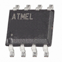
ATTINY25-20SH Atmel, ATTINY25-20SH Datasheet - Page 110

ATTINY25-20SH
Manufacturer Part Number
ATTINY25-20SH
Description
IC MCU AVR 2KB FLASH 20MHZ 8SOIC
Manufacturer
Atmel
Series
AVR® ATtinyr
Datasheet
1.ATTINY25-20MU.pdf
(236 pages)
Specifications of ATTINY25-20SH
Core Processor
AVR
Core Size
8-Bit
Speed
20MHz
Connectivity
USI
Peripherals
Brown-out Detect/Reset, POR, PWM, WDT
Number Of I /o
6
Program Memory Size
2KB (1K x 16)
Program Memory Type
FLASH
Eeprom Size
128 x 8
Ram Size
128 x 8
Voltage - Supply (vcc/vdd)
2.7 V ~ 5.5 V
Data Converters
A/D 4x10b
Oscillator Type
Internal
Operating Temperature
-40°C ~ 85°C
Package / Case
8-SOIC (5.3mm Width), 8-SOP, 8-SOEIAJ
Processor Series
ATtiny
Core
AVR
Data Bus Width
8 bit
Data Ram Size
128 B
Interface Type
SPI, USI
Maximum Clock Frequency
20 MHz
Number Of Programmable I/os
6
Number Of Timers
2
Operating Supply Voltage
5 V
Maximum Operating Temperature
+ 85 C
Mounting Style
SMD/SMT
3rd Party Development Tools
EWAVR, EWAVR-BL
Development Tools By Supplier
ATAVRDRAGON, ATSTK500, ATSTK600, ATAVRISP2, ATAVRONEKIT
Minimum Operating Temperature
- 40 C
Operating Temperature Range
- 40 C to + 85 C
Lead Free Status / RoHS Status
Lead free / RoHS Compliant
- Current page: 110 of 236
- Download datasheet (5Mb)
14.1.2
14.1.3
110
ATtiny25/45/85
DT1A – Timer/Counter1 Dead Time A
DT1B – Timer/Counter1 Dead Time B
The dead time value register A is an 8-bit read/write register.
The dead time delay of is adjusted by the dead time value register, DT1A. The register consists
of two fields, DT1AH[3:0] and DT1AL[3:0], one for each complementary output. Therefore a dif-
ferent dead time delay can be adjusted for the rising edge of OC1A and the rising edge of OC1A.
• Bits 7:4 – DT1AH[3:0]: Dead Time Value for OC1A Output
The dead time value for the OC1A output. The dead time delay is set as a number of the pres-
caled timer/counter clocks. The minimum dead time is zero and the maximum dead time is the
prescaled time/counter clock period multiplied by 15.
• Bits 3:0 – DT1AL[3:0]: Dead Time Value for OC1A Output
The dead time value for the OC1A output. The dead time delay is set as a number of the pres-
caled timer/counter clocks. The minimum dead time is zero and the maximum dead time is the
prescaled time/counter clock period multiplied by 15.
The dead time value register Bis an 8-bit read/write register.
The dead time delay of is adjusted by the dead time value register, DT1B. The register consists
of two fields, DT1BH[3:0] and DT1BL[3:0], one for each complementary output. Therefore a dif-
ferent dead time delay can be adjusted for the rising edge of OC1A and the rising edge of OC1A.
• Bits 7:4 – DT1BH[3:0]: Dead Time Value for OC1B Output
The dead time value for the OC1B output. The dead time delay is set as a number of the pres-
caled timer/counter clocks. The minimum dead time is zero and the maximum dead time is the
prescaled time/counter clock period multiplied by 15.
• Bits 3:0 – DT1BL[3:0]: Dead Time Value for OC1B Output
The dead time value for the OC1B output. The dead time delay is set as a number of the pres-
caled timer/counter clocks. The minimum dead time is zero and the maximum dead time is the
prescaled time/counter clock period multiplied by 15.
Bit
0x25
Read/Write
Initial value
Bit
0x24
Read/Write
Initial value
DT1AH3
DT1BH3
R/W
R/W
7
0
7
0
DT1AH2
DT1BH2
R/W
R/W
6
0
6
0
DT1AH1
DT1BH1
R/W
R/W
5
0
5
0
DT1AH0
DT1BH0
R/W
R/W
4
0
4
0
DT1AL3
DT1BL3
R/W
R/W
3
0
3
0
DT1AL2
DT1BL2
R/W
R/W
2
0
2
0
DT1AL1
DT1BL1
R/W
R/W
1
0
1
0
DT1AL0
DT1BL0
R/W
R/W
0
0
0
0
2586M–AVR–07/10
DT1A
DT1B
Related parts for ATTINY25-20SH
Image
Part Number
Description
Manufacturer
Datasheet
Request
R

Part Number:
Description:
Manufacturer:
Atmel Corporation
Datasheet:

Part Number:
Description:
Manufacturer:
Atmel Corporation
Datasheet:

Part Number:
Description:
IC MCU AVR 2K FLASH 20MHZ 20-QFN
Manufacturer:
Atmel
Datasheet:

Part Number:
Description:
IC AVR MCU 2K 20MHZ 8-DIP
Manufacturer:
Atmel
Datasheet:

Part Number:
Description:
IC AVR MCU 2K 20MHZ 8-SOIC
Manufacturer:
Atmel
Datasheet:

Part Number:
Description:
MCU AVR 2K FLASH 15MHZ 20-QFN
Manufacturer:
Atmel
Datasheet:

Part Number:
Description:
8-bit Microcontrollers - MCU AVR 16KB FL 512B EE 1KB SRAM 10 MHZ GRN
Manufacturer:
Atmel

Part Number:
Description:
8-bit Microcontrollers - MCU AVR 16KB FL 512B EE 1KB SRAM 10 MHZ GRN
Manufacturer:
Atmel

Part Number:
Description:
MCU AVR 2K ISP FLASH 2.7V 8-SOIC
Manufacturer:
Atmel
Datasheet:

Part Number:
Description:
MCU AVR 2KB FLASH 20MHZ 8SOIC
Manufacturer:
Atmel
Datasheet:

Part Number:
Description:
IC MCU AVR 2KB FLASH 20MHZ 8SOIC
Manufacturer:
Atmel
Datasheet:

Part Number:
Description:
MCU AVR 2KB FLASH 20MHZ 8SOIC
Manufacturer:
Atmel
Datasheet:

Part Number:
Description:
MCU AVR 2KB FLASH 20MHZ 8SOIC
Manufacturer:
Atmel
Datasheet:

Part Number:
Description:
MCU AVR 2KB FLASH 20MHZ 20QFN
Manufacturer:
Atmel
Datasheet:


