ATTINY24-15MZ Atmel, ATTINY24-15MZ Datasheet - Page 166
ATTINY24-15MZ
Manufacturer Part Number
ATTINY24-15MZ
Description
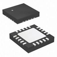
MCU AVR 2K FLASH 15MHZ 20-QFN
Manufacturer
Atmel
Series
AVR® ATtinyr
Datasheet
1.ATTINY24-15MZ.pdf
(225 pages)
Specifications of ATTINY24-15MZ
Package / Case
20-QFN Exposed Pad
Voltage - Supply (vcc/vdd)
2.7 V ~ 5.5 V
Operating Temperature
-40°C ~ 125°C
Speed
16MHz
Number Of I /o
12
Eeprom Size
128 x 8
Core Processor
AVR
Program Memory Type
FLASH
Ram Size
128 x 8
Program Memory Size
2KB (2K x 8)
Data Converters
A/D 8x10b
Oscillator Type
Internal
Peripherals
Brown-out Detect/Reset, POR, PWM, WDT
Connectivity
USI
Core Size
8-Bit
Cpu Family
ATtiny
Device Core
AVR
Device Core Size
8b
Frequency (max)
16MHz
Interface Type
SPI/UART
Total Internal Ram Size
128Byte
# I/os (max)
12
Number Of Timers - General Purpose
2
Operating Supply Voltage (typ)
3.3/5V
Operating Supply Voltage (max)
5.5V
Operating Supply Voltage (min)
2.7V
On-chip Adc
8-chx10-bit
Instruction Set Architecture
RISC
Operating Temp Range
-40C to 125C
Operating Temperature Classification
Automotive
Mounting
Surface Mount
Pin Count
20
Package Type
QFN EP
Lead Free Status / RoHS Status
Lead free / RoHS Compliant


21.6
166
Serial Downloading
Atmel ATtiny24/44/84 [Preliminary]
Both the Flash and EEPROM memory arrays can be programmed using the serial SPI bus
while RESET is pulled to GND. The serial interface consists of pins SCK, MOSI (input) and
MISO (output). After RESET is set low, the Programming Enable instruction needs to be exe-
cuted first before program/erase operations can be executed. NOTE, in
166, the pin mapping for SPI programming is listed. Not all parts use the SPI pins dedicated
for the internal SPI interface.
Figure 21-1. Serial Programming and Verify
Note:
Table 21-9.
When programming the EEPROM, an auto-erase cycle is built into the self-timed program-
ming operation (in serial mode only), and there is no need to first execute the chip erase
instruction. The chip erase operation turns the content of every memory location in both the
program and EEPROM arrays into 0xFF.
Depending on the CKSEL fuses, a valid clock must be present. The minimum low and high
periods for the serial clock (SCK) input are defined as follows:
Low: > 2 CPU clock cycles for f
High: > 2 CPU clock cycles for f
1. If the device is clocked by the internal oscillator, it is not needed to connect a clock source to
Symbol
MOSI
MISO
SCK
the CLKI pin.
Pin Mapping Serial Programming
MOSI
MISO
SCK
ck
ck
Pins
PA6
PA5
PA4
< 12MHz, 3 CPU clock cycles for f
< 12MHz, 3 CPU clock cycles for f
RESET
GND
(1)
VCC
I/O
O
I
I
+1.8 - 5.5V
ck
ck
>= 12MHz
>= 12MHz
Description
Serial Data in
Serial Data out
Serial Clock
Table 21-9 on page
7701D–AVR–09/10
Related parts for ATTINY24-15MZ
Image
Part Number
Description
Manufacturer
Datasheet
Request
R

Part Number:
Description:
Manufacturer:
Atmel Corporation
Datasheet:
Part Number:
Description:
Manufacturer:
Atmel Corporation
Datasheet:

Part Number:
Description:
IC MCU AVR 2K FLASH 20MHZ 20-QFN
Manufacturer:
Atmel
Datasheet:

Part Number:
Description:
IC MCU AVR 2K FLASH 20MHZ 14SOIC
Manufacturer:
Atmel
Datasheet:

Part Number:
Description:
IC MCU AVR 2K FLASH 20MHZ 14-DIP
Manufacturer:
Atmel
Datasheet:

Part Number:
Description:
MCU AVR 2KB FLASH 20MHZ 14SOIC
Manufacturer:
Atmel
Datasheet:
Part Number:
Description:
MCU AVR 2KB FLASH 20MHZ 20QFN
Manufacturer:
Atmel
Datasheet:
Part Number:
Description:
MCU AVR 2K FLASH 15MHZ 14-SOIC
Manufacturer:
Atmel
Datasheet:

Part Number:
Description:
DEV KIT FOR AVR/AVR32
Manufacturer:
Atmel
Datasheet:
Part Number:
Description:
INTERVAL AND WIPE/WASH WIPER CONTROL IC WITH DELAY
Manufacturer:
ATMEL Corporation
Datasheet:
Part Number:
Description:
Low-Voltage Voice-Switched IC for Hands-Free Operation
Manufacturer:
ATMEL Corporation
Datasheet:
Part Number:
Description:
MONOLITHIC INTEGRATED FEATUREPHONE CIRCUIT
Manufacturer:
ATMEL Corporation
Datasheet: