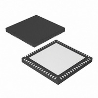
DSPIC33FJ64GS606T-I/MR Microchip Technology, DSPIC33FJ64GS606T-I/MR Datasheet - Page 117

DSPIC33FJ64GS606T-I/MR
Manufacturer Part Number
DSPIC33FJ64GS606T-I/MR
Description
MCU/DSP 16BIT 64KB FLASH 64QFN
Manufacturer
Microchip Technology
Series
dsPIC™ 33Fr
Datasheet
1.DSPIC33FJ32GS406-IPT.pdf
(418 pages)
Specifications of DSPIC33FJ64GS606T-I/MR
Program Memory Type
FLASH
Program Memory Size
64KB (64K x 8)
Package / Case
64-VFQFN, Exposed Pad
Core Processor
dsPIC
Core Size
16-Bit
Speed
40 MIPs
Connectivity
CAN, I²C, IrDA, LIN, SPI, UART/USART, USB
Peripherals
Brown-out Detect/Reset, DMA, QEI, POR, PWM, WDT
Number Of I /o
58
Ram Size
9K x 8
Voltage - Supply (vcc/vdd)
3 V ~ 3.6 V
Data Converters
A/D 16x10b; D/A 1x10b
Oscillator Type
Internal
Operating Temperature
-40°C ~ 85°C
Product
DSCs
Data Bus Width
16 bit
Processor Series
DSPIC33F
Core
dsPIC
Numeric And Arithmetic Format
Fixed-Point or Floating-Point
Instruction Set Architecture
Harvard
Device Million Instructions Per Second
40 MIPs
Maximum Clock Frequency
120 MHz
Number Of Programmable I/os
58
Data Ram Size
4 KB
Operating Supply Voltage
3.3 V
Maximum Operating Temperature
+ 85 C
Mounting Style
SMD/SMT
3rd Party Development Tools
52713-733, 52714-737, 53276-922, EWDSPIC
Development Tools By Supplier
PG164130, DV164035, DV244005, DV164005, PG164120, DM240001, DV164033
Interface Type
I2C, SPI, UART
Minimum Operating Temperature
- 40 C
On-chip Adc
10 bit, 16 Channel
On-chip Dac
10 bit, 4 Channel
Lead Free Status / RoHS Status
Lead free / RoHS Compliant
Eeprom Size
-
Lead Free Status / Rohs Status
Lead free / RoHS Compliant
- Current page: 117 of 418
- Download datasheet (3Mb)
6.1
The
dsPIC33FJ64GS406/606/608/610 families of devices
have two types of Reset:
• Cold Reset
• Warm Reset
A cold Reset is the result of a Power-on Reset (POR)
or a Brown-out Reset (BOR). On a cold Reset, the
FNOSC Configuration bits in the FOSC Configuration
register select the device clock source.
A warm Reset is the result of all the other Reset
sources, including the RESET instruction. On warm
Reset, the device will continue to operate from the
current clock source as indicated by the Current
Oscillator Selection (COSC<2:0>) bits in the Oscillator
Control (OSCCON<14:12>) register.
The device is kept in a Reset state until the system
power supplies have stabilized at appropriate levels
and the oscillator clock is ready. The sequence in
which this occurs is detailed below and is shown in
Figure 6-2.
1.
TABLE 6-1:
2010 Microchip Technology Inc.
FRC, FRCDIV16, FRCDIVN
FRCPLL
XT
HS
EC
XTPLL
HSPLL
ECPLL
LPRC
Note 1:
dsPIC33FJ32GS406/606/608/610 and dsPIC33FJ64GS406/606/608/610
POR Reset: A POR circuit holds the device in
Reset when the power supply is turned on. The
POR circuit is active until V
threshold and the delay, T
Oscillator Mode
2:
3:
System Reset
dsPIC33FJ32GS406/606/608/610
T
times vary with crystal characteristics, load capacitance, etc.
T
10 MHz crystal and T
T
OSCD
OST
LOCK
= Oscillator start-up timer delay (1024 oscillator clock period). For example, T
OSCILLATOR DELAY
= Oscillator start-up delay (1.1 s max for FRC, 70 s max for LPRC). Crystal oscillator start-up
= PLL lock time (1.5 ms nominal) if PLL is enabled.
POR
DD
OST
Start-up Delay
, has elapsed.
crosses the V
Oscillator
T
T
T
T
T
T
T
= 32 ms for a 32 kHz crystal.
OSCD
OSCD
OSCD
OSCD
OSCD
OSCD
OSCD
—
—
(1)
(1)
(1)
(1)
(1)
(1)
(1)
POR
and
Preliminary
Start-up Timer
Oscillator
T
T
T
T
OST
OST
OST
OST
—
—
—
—
—
2.
3.
4.
5.
6.
(2)
(2)
(2)
(2)
BOR Reset: The on-chip voltage regulator has
a BOR circuit that keeps the device in Reset
until V
delay, T
ensures that the voltage regulator output
becomes stable.
PWRT Timer: The programmable power-up
timer continues to hold the processor in Reset
for a specific period of time (T
BOR. The delay T
power
appropriate level for full-speed operation. After
the delay, T
becomes inactive, which in turn enables the
selected oscillator to start generating clock
cycles.
Oscillator Delay: The total delay for the clock to
be ready for various clock source selections is
given
“Oscillator Configuration” for more information.
When the oscillator clock is ready, the processor
begins execution from location 0x000000. The
user application programs a GOTO instruction at
the Reset address, which redirects program
execution to the appropriate start-up routine.
The Fail-Safe Clock Monitor (FSCM), if enabled,
begins to monitor the system clock when the
system clock is ready and the delay, T
elapsed.
DD
in
BOR
PLL Lock Time
supplies
crosses the V
Table 6-1.
, has elapsed. The delay, T
T
T
T
T
PWRT
LOCK
LOCK
LOCK
LOCK
—
—
—
—
—
PWRT
, has elapsed, the SYSRST
(3)
(3)
(3)
(3)
have
ensures that the system
Refer
BOR
OST
stabilized
T
threshold and the
T
T
OSCD
= 102.4 s for a
DS70591C-page 117
T
T
OSCD
OSCD
to
OSCD
OSCD
Total Delay
T
T
PWRT
LOCK
LOCK
T
T
T
OSCD
OSCD
LOCK
Section 9.0
+ T
+ T
+ T
—
+ T
+ T
) after a
(1,2,3)
(1,2,3)
LOCK
at
OST
OST
(1)
(3)
(1)
OST
OST
FSCM
BOR
(1,2)
(1,2)
the
(1,3)
+
+
,
,
Related parts for DSPIC33FJ64GS606T-I/MR
Image
Part Number
Description
Manufacturer
Datasheet
Request
R

Part Number:
Description:
Manufacturer:
Microchip Technology Inc.
Datasheet:

Part Number:
Description:
Manufacturer:
Microchip Technology Inc.
Datasheet:

Part Number:
Description:
Manufacturer:
Microchip Technology Inc.
Datasheet:

Part Number:
Description:
Manufacturer:
Microchip Technology Inc.
Datasheet:

Part Number:
Description:
Manufacturer:
Microchip Technology Inc.
Datasheet:

Part Number:
Description:
Manufacturer:
Microchip Technology Inc.
Datasheet:

Part Number:
Description:
Manufacturer:
Microchip Technology Inc.
Datasheet:

Part Number:
Description:
Manufacturer:
Microchip Technology Inc.
Datasheet:


