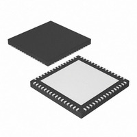
DSPIC33FJ64GS606T-I/MR Microchip Technology, DSPIC33FJ64GS606T-I/MR Datasheet - Page 353

DSPIC33FJ64GS606T-I/MR
Manufacturer Part Number
DSPIC33FJ64GS606T-I/MR
Description
MCU/DSP 16BIT 64KB FLASH 64QFN
Manufacturer
Microchip Technology
Series
dsPIC™ 33Fr
Datasheet
1.DSPIC33FJ32GS406-IPT.pdf
(418 pages)
Specifications of DSPIC33FJ64GS606T-I/MR
Program Memory Type
FLASH
Program Memory Size
64KB (64K x 8)
Package / Case
64-VFQFN, Exposed Pad
Core Processor
dsPIC
Core Size
16-Bit
Speed
40 MIPs
Connectivity
CAN, I²C, IrDA, LIN, SPI, UART/USART, USB
Peripherals
Brown-out Detect/Reset, DMA, QEI, POR, PWM, WDT
Number Of I /o
58
Ram Size
9K x 8
Voltage - Supply (vcc/vdd)
3 V ~ 3.6 V
Data Converters
A/D 16x10b; D/A 1x10b
Oscillator Type
Internal
Operating Temperature
-40°C ~ 85°C
Product
DSCs
Data Bus Width
16 bit
Processor Series
DSPIC33F
Core
dsPIC
Numeric And Arithmetic Format
Fixed-Point or Floating-Point
Instruction Set Architecture
Harvard
Device Million Instructions Per Second
40 MIPs
Maximum Clock Frequency
120 MHz
Number Of Programmable I/os
58
Data Ram Size
4 KB
Operating Supply Voltage
3.3 V
Maximum Operating Temperature
+ 85 C
Mounting Style
SMD/SMT
3rd Party Development Tools
52713-733, 52714-737, 53276-922, EWDSPIC
Development Tools By Supplier
PG164130, DV164035, DV244005, DV164005, PG164120, DM240001, DV164033
Interface Type
I2C, SPI, UART
Minimum Operating Temperature
- 40 C
On-chip Adc
10 bit, 16 Channel
On-chip Dac
10 bit, 4 Channel
Lead Free Status / RoHS Status
Lead free / RoHS Compliant
Eeprom Size
-
Lead Free Status / Rohs Status
Lead free / RoHS Compliant
- Current page: 353 of 418
- Download datasheet (3Mb)
27.0
This section provides an overview of dsPIC33FJ32GS406/606/608/610 and dsPIC33FJ64GS406/606/608/610 electri-
cal characteristics. Additional information will be provided in future revisions of this document as it becomes available.
Absolute maximum ratings for the dsPIC33FJ32GS406/606/608/610 and dsPIC33FJ64GS406/606/608/610 family are
listed below. Exposure to these maximum rating conditions for extended periods may affect device reliability. Functional
operation of the device at these or any other conditions above the parameters indicated in the operation listings of this
specification is not implied.
Absolute Maximum Ratings
Ambient temperature under bias.............................................................................................................-40°C to +125°C
Storage temperature .............................................................................................................................. -65°C to +150°C
Voltage on V
Voltage on any pin that is not 5V tolerant, with respect to V
Voltage on any 5V tolerant pin with respect to V
Voltage on any 5V tolerant pin with respect to Vss, when V
Voltage on V
Maximum current out of V
Maximum current into V
Maximum output current sunk by any I/O pin
Maximum output current sourced by any I/O pin
Maximum current sunk by all ports .......................................................................................................................200 mA
Maximum current sourced by all ports
Maximum output current sunk by non-remappable PWM pins ...............................................................................16 mA
Maximum output current sourced by non-remappable PWM pins ..........................................................................16 mA
2010 Microchip Technology Inc.
dsPIC33FJ32GS406/606/608/610 and dsPIC33FJ64GS406/606/608/610
Note 1: Stresses above those listed under “Absolute Maximum Ratings” may cause permanent damage to the
2: Maximum allowable current is a function of device maximum power dissipation (see Table 27-2).
3: Exceptions are PWMxL, and PWMxH, which are able to sink/source 16 mA, and digital pins, which are able
4: See the “Pin Diagrams” section for 5V tolerant pins.
ELECTRICAL CHARACTERISTICS
device. This is a stress rating only, and functional operation of the device at those or any other conditions
above those indicated in the operation listings of this specification is not implied. Exposure to maximum
rating conditions for extended periods may affect device reliability.
to sink/source 8 mA.
DD
CAP
with respect to V
/V
DDCORE
DD
SS
with respect to V
pin
pin ...........................................................................................................................300 mA
(2)
...........................................................................................................................250 mA
SS
(1)
......................................................................................................... -0.3V to +4.0V
(2)
...............................................................................................................200 mA
SS
(3)
....................................................................................... 2.25V to 2.75V
........................................................................................................4 mA
SS
(3)
, when Vdd 3.0V
...................................................................................................4 mA
Preliminary
SS
DD
(4)
< 3.0V
................................................... -0.3V to (V
(4)
(4)
........................................ -0.3V to (V
................................................. -0.3V to +5.6V
DS70591C-page 353
DD
DD
+ 0.3V)
+ 0.3V)
Related parts for DSPIC33FJ64GS606T-I/MR
Image
Part Number
Description
Manufacturer
Datasheet
Request
R

Part Number:
Description:
Manufacturer:
Microchip Technology Inc.
Datasheet:

Part Number:
Description:
Manufacturer:
Microchip Technology Inc.
Datasheet:

Part Number:
Description:
Manufacturer:
Microchip Technology Inc.
Datasheet:

Part Number:
Description:
Manufacturer:
Microchip Technology Inc.
Datasheet:

Part Number:
Description:
Manufacturer:
Microchip Technology Inc.
Datasheet:

Part Number:
Description:
Manufacturer:
Microchip Technology Inc.
Datasheet:

Part Number:
Description:
Manufacturer:
Microchip Technology Inc.
Datasheet:

Part Number:
Description:
Manufacturer:
Microchip Technology Inc.
Datasheet:


