PIC24FJ256GB206-I/MR Microchip Technology, PIC24FJ256GB206-I/MR Datasheet - Page 177
PIC24FJ256GB206-I/MR
Manufacturer Part Number
PIC24FJ256GB206-I/MR
Description
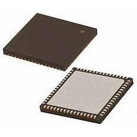
MCU PIC 16BIT FLASH 256K 64VQFN
Manufacturer
Microchip Technology
Series
PIC® 24Fr
Specifications of PIC24FJ256GB206-I/MR
Core Size
16-Bit
Program Memory Size
256KB (85.5K x 24)
Core Processor
PIC
Speed
32MHz
Connectivity
I²C, IrDA, SPI, UART/USART, USB OTG
Peripherals
Brown-out Detect/Reset, LVD, POR, PWM, WDT
Number Of I /o
52
Program Memory Type
FLASH
Ram Size
96K x 8
Voltage - Supply (vcc/vdd)
2.2 V ~ 3.6 V
Data Converters
A/D 16x10b
Oscillator Type
Internal
Operating Temperature
-40°C ~ 85°C
Package / Case
64-VFQFN, Exposed Pad
Controller Family/series
PIC24
No. Of I/o's
52
Ram Memory Size
96KB
Cpu Speed
32MHz
No. Of Timers
5
No. Of Pwm Channels
9
Processor Series
PIC24FJ
Core
PIC
Data Bus Width
16 bit
Data Ram Size
96 KB
Interface Type
I2C, SPI, UART
Maximum Clock Frequency
32 MHz
Number Of Programmable I/os
29
Number Of Timers
5
Operating Supply Voltage
2.2 V to 3.6 V
Maximum Operating Temperature
+ 85 C
Mounting Style
SMD/SMT
3rd Party Development Tools
52713-733, 52714-737, 53276-922, EWDSPIC
Development Tools By Supplier
PG164130, DV164035, DV244005, DV164005, DM240001, MA240021
Minimum Operating Temperature
- 40 C
On-chip Adc
10 bit, 16 Channel
Lead Free Status / RoHS Status
Lead free / RoHS Compliant
Eeprom Size
-
Lead Free Status / Rohs Status
Details


REGISTER 10-35: RPOR6: PERIPHERAL PIN SELECT OUTPUT REGISTER 6
REGISTER 10-36: RPOR7: PERIPHERAL PIN SELECT OUTPUT REGISTER 7
2010 Microchip Technology Inc.
bit 15
bit 7
Legend:
R = Readable bit
-n = Value at POR
bit 15-14
bit 13-8
bit 7-6
bit 5-0
bit 15
bit 7
Legend:
R = Readable bit
-n = Value at POR
bit 15-14
bit 13-8
bit 7-6
bit 5-0
Note 1:
U-0
U-0
U-0
U-0
—
—
—
—
Unimplemented in 64-pin devices; read as ‘0’.
Unimplemented: Read as ‘0’
RP13R<5:0>: RP13 Output Pin Mapping bits
Peripheral output number n is assigned to pin, RP13 (see Table 10-4 for peripheral function numbers).
Unimplemented: Read as ‘0’
RP12R<5:0>: RP12 Output Pin Mapping bits
Peripheral output number n is assigned to pin, RP12 (see Table 10-4 for peripheral function numbers).
Unimplemented: Read as ‘0’
RP15R<5:0>: RP15 Output Pin Mapping bits
Peripheral output number n is assigned to pin, RP0 (see Table 10-4 for peripheral function numbers).
Unimplemented: Read as ‘0’
RP14R<5:0>: RP14 Output Pin Mapping bits
Peripheral output number n is assigned to pin, RP14 (see Table 10-4 for peripheral function numbers).
U-0
U-0
U-0
U-0
—
—
—
—
W = Writable bit
‘1’ = Bit is set
W = Writable bit
‘1’ = Bit is set
RP15R5
RP13R5
RP12R5
RP14R5
R/W-0
R/W-0
R/W-0
R/W-0
(1)
RP15R4
PIC24FJ256GB210 FAMILY
RP13R4
RP12R4
RP14R4
R/W-0
R/W-0
R/W-0
R/W-0
(1)
U = Unimplemented bit, read as ‘0’
‘0’ = Bit is cleared
U = Unimplemented bit, read as ‘0’
‘0’ = Bit is cleared
(1)
RP15R3
RP13R3
RP12R3
RP14R3
R/W-0
R/W-0
R/W-0
R/W-0
(1)
RP15R2
RP13R2
RP12R2
RP14R2
R/W-0
R/W-0
R/W-0
R/W-0
(1)
x = Bit is unknown
x = Bit is unknown
RP15R1
RP13R1
RP12R1
RP14R1
R/W-0
R/W-0
R/W-0
R/W-0
(1)
DS39975A-page 177
RP15R0
RP13R0
RP12R0
RP14R0
R/W-0
R/W-0
R/W-0
R/W-0
bit 8
bit 0
bit 8
bit 0
(1)
Related parts for PIC24FJ256GB206-I/MR
Image
Part Number
Description
Manufacturer
Datasheet
Request
R

Part Number:
Description:
Manufacturer:
Microchip Technology Inc.
Datasheet:
Part Number:
Description:
Manufacturer:
Microchip Technology Inc.
Datasheet:
Part Number:
Description:
Manufacturer:
Microchip Technology Inc.
Datasheet:
Part Number:
Description:
Manufacturer:
Microchip Technology Inc.
Datasheet:
Part Number:
Description:
Manufacturer:
Microchip Technology Inc.
Datasheet:
Part Number:
Description:
Manufacturer:
Microchip Technology Inc.
Datasheet:
Part Number:
Description:
Manufacturer:
Microchip Technology Inc.
Datasheet:
Part Number:
Description:
Manufacturer:
Microchip Technology Inc.
Datasheet: