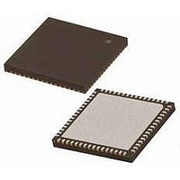
PIC24FJ256GB206-I/MR Microchip Technology, PIC24FJ256GB206-I/MR Datasheet - Page 269

PIC24FJ256GB206-I/MR
Manufacturer Part Number
PIC24FJ256GB206-I/MR
Description
MCU PIC 16BIT FLASH 256K 64VQFN
Manufacturer
Microchip Technology
Series
PIC® 24Fr
Specifications of PIC24FJ256GB206-I/MR
Core Size
16-Bit
Program Memory Size
256KB (85.5K x 24)
Core Processor
PIC
Speed
32MHz
Connectivity
I²C, IrDA, SPI, UART/USART, USB OTG
Peripherals
Brown-out Detect/Reset, LVD, POR, PWM, WDT
Number Of I /o
52
Program Memory Type
FLASH
Ram Size
96K x 8
Voltage - Supply (vcc/vdd)
2.2 V ~ 3.6 V
Data Converters
A/D 16x10b
Oscillator Type
Internal
Operating Temperature
-40°C ~ 85°C
Package / Case
64-VFQFN, Exposed Pad
Controller Family/series
PIC24
No. Of I/o's
52
Ram Memory Size
96KB
Cpu Speed
32MHz
No. Of Timers
5
No. Of Pwm Channels
9
Processor Series
PIC24FJ
Core
PIC
Data Bus Width
16 bit
Data Ram Size
96 KB
Interface Type
I2C, SPI, UART
Maximum Clock Frequency
32 MHz
Number Of Programmable I/os
29
Number Of Timers
5
Operating Supply Voltage
2.2 V to 3.6 V
Maximum Operating Temperature
+ 85 C
Mounting Style
SMD/SMT
3rd Party Development Tools
52713-733, 52714-737, 53276-922, EWDSPIC
Development Tools By Supplier
PG164130, DV164035, DV244005, DV164005, DM240001, MA240021
Minimum Operating Temperature
- 40 C
On-chip Adc
10 bit, 16 Channel
Lead Free Status / RoHS Status
Lead free / RoHS Compliant
Eeprom Size
-
Lead Free Status / Rohs Status
Details
- Current page: 269 of 386
- Download datasheet (4Mb)
19.0
The Enhanced Parallel Master Port (EPMP) module
provides a parallel 4-bit (Master mode only), 8-bit (Mas-
ter and Slave modes) or 16-bit (Master mode only) data
bus interface to communicate with off-chip modules,
such as memories, FIFOs, LCD controllers and other
microcontrollers. This module can serve as either the
master or the slave on the communication bus. For
EPMP Master modes, all external addresses are
mapped into the internal Extended Data Space (EDS).
This is done by allocating a region of the EDS for each
chip select, and then assigning each chip select to a
particular external resource, such as a memory or
external controller. This region should not be assigned
to another device resource, such as RAM or SFRs. To
perform a write or read on an external resource, the
CPU should simply perform a write or read within the
address range assigned for EPMP.
TABLE 19-1:
2010 Microchip Technology Inc.
Note 1:
Note:
ENHANCED PARALLEL
MASTER PORT (EPMP)
RA14
RF12
RG6
RG7
RG8
RC4
RA3
RA4
Pin
The alternate EPMP pins are valid only for 100-pin devices (PIC24FJXXXGB210).
This data sheet summarizes the features
of this group of PIC24F devices. It is not
intended to be a comprehensive reference
source. For more information, refer to the
“PIC24F
Section 42. “Enhanced Parallel Master
Port (EPMP)” (DS39730). The informa-
tion in this data sheet supersedes the
information in the FRM.
ALTERNATE EPMP PINS
Family
Reference
ALTPMP = 0
PMCS2
PMA22
PMA18
PMA20
PMA21
PMA5
PMA4
PMA3
Manual”,
PIC24FJ256GB210 FAMILY
(1)
Key features of the EPMP module are:
• Extended Data Space (EDS) Interface allows
• Up to 23 Programmable Address Lines
• Up to 2 Chip Select Lines
• Up to 2 Acknowledgement Lines (one per chip
• 4-Bit, 8-Bit or 16-Bit Wide Data Bus
• Programmable Strobe Options (per chip select)
• Programmable Address/Data Multiplexing
• Programmable Address Wait States
• Programmable Data Wait States (per chip select)
• Programmable Polarity on Control Signals (per
• Legacy Parallel Slave Port Support
• Enhanced Parallel Slave Support
19.1
Many of the lower order EPMP address pins are shared
with ADC inputs. This is an untenable situation for
users that need both the ADC channels and the EPMP
bus. If the user does not need to use all the address
bits, then by clearing the ALTPMP (CW3<12>) Config-
uration bit, the lower order address bits can be mapped
to higher address pins, which frees the ADC channels.
Direct Access from the CPU
select)
- Individual Read and Write Strobes or;
- Read/Write Strobe with Enable Strobe
chip select)
- Address Support
- 4-Byte Deep Auto-Incrementing Buffer
Note:
ALTPMP Setting
The alternate PMP pin selection is not
available
(PIC24FJXXXGB206)
Configuration bit, ALTPMP, is also not
available.
ALTPMP = 1
in
PMCS2
PMA22
PMA18
PMA20
PMA21
PMA5
PMA4
PMA3
64-pin
DS39975A-page 269
and
so
devices
the
Related parts for PIC24FJ256GB206-I/MR
Image
Part Number
Description
Manufacturer
Datasheet
Request
R

Part Number:
Description:
Manufacturer:
Microchip Technology Inc.
Datasheet:

Part Number:
Description:
Manufacturer:
Microchip Technology Inc.
Datasheet:

Part Number:
Description:
Manufacturer:
Microchip Technology Inc.
Datasheet:

Part Number:
Description:
Manufacturer:
Microchip Technology Inc.
Datasheet:

Part Number:
Description:
Manufacturer:
Microchip Technology Inc.
Datasheet:

Part Number:
Description:
Manufacturer:
Microchip Technology Inc.
Datasheet:

Part Number:
Description:
Manufacturer:
Microchip Technology Inc.
Datasheet:

Part Number:
Description:
Manufacturer:
Microchip Technology Inc.
Datasheet:


