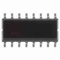
ST7FLITES2Y0M6 STMicroelectronics, ST7FLITES2Y0M6 Datasheet - Page 73

ST7FLITES2Y0M6
Manufacturer Part Number
ST7FLITES2Y0M6
Description
MCU 8BIT 1K FLASH 16SOIC
Manufacturer
STMicroelectronics
Series
ST7r
Datasheet
1.ST7FLITES2Y0B6.pdf
(124 pages)
Specifications of ST7FLITES2Y0M6
Core Processor
ST7
Core Size
8-Bit
Speed
8MHz
Connectivity
SPI
Peripherals
LVD, POR, PWM, WDT
Number Of I /o
13
Program Memory Size
1KB (1K x 8)
Program Memory Type
FLASH
Ram Size
128 x 8
Voltage - Supply (vcc/vdd)
2.4 V ~ 5.5 V
Oscillator Type
Internal
Operating Temperature
-40°C ~ 85°C
Package / Case
16-SOIC (3.9mm Width)
Controller Family/series
ST7
No. Of I/o's
13
Ram Memory Size
128Byte
Cpu Speed
8MHz
No. Of Timers
2
Embedded Interface Type
SPI
No. Of Pwm Channels
1
Rohs Compliant
Yes
Processor Series
ST7FLITESx
Core
ST7
Data Bus Width
8 bit
Data Ram Size
128 B
Interface Type
SPI
Maximum Clock Frequency
8 MHz
Number Of Programmable I/os
13
Number Of Timers
2
Operating Supply Voltage
2.4 V to 5.5 V
Maximum Operating Temperature
+ 85 C
Mounting Style
SMD/SMT
Development Tools By Supplier
ST7FLIT0-IND/USB, ST7FLITE-SK/RAIS, ST7MDT10-DVP3, ST7MDT10-EMU3, STX-RLINK
Minimum Operating Temperature
- 40 C
On-chip Adc
8 bit
For Use With
497-5858 - EVAL BOARD PLAYBACK ST7FLITE497-5049 - KIT STARTER RAISONANCE ST7FLITE
Lead Free Status / RoHS Status
Lead free / RoHS Compliant
Eeprom Size
-
Data Converters
-
Lead Free Status / Rohs Status
In Transition
Other names
497-4861
Available stocks
Company
Part Number
Manufacturer
Quantity
Price
8-BIT A/D CONVERTER (ADC) (Cont’d)
11.4.6 Register Description
CONTROL/STATUS REGISTER (ADCCSR)
Read/Write
Reset Value: 0000 0000 (00h)
Bit 7 = EOC Conversion Complete
This bit is set by hardware. It is cleared by soft-
ware reading the result in the DR register or writing
to the CSR register.
0: Conversion is not complete
1: Conversion can be read from the DR register
Bit 6 = SPEED ADC clock selection
This bit is set and cleared by software. It is used
together with the SLOW bit to configure the ADC
clock speed. Refer to the table in the SLOW bit de-
scription.
Bit 5 = ADON A/D Converter and Amplifier On
This bit is set and cleared by software.
0: A/D converter and amplifier are switched off
1: A/D converter and amplifier are switched on
Note: Amplifier not available on ST7LITES5
devices
Bits 4:3 = Reserved. must always be cleared.
Bits 2:0 = CH[2:0] Channel Selection
These bits are set and cleared by software. They
select the analog input to convert.
Notes:
1. The number of pins AND the channel selection
varies according to the device. Refer to the device
pinout.
2. A write to the ADCCSR register (with ADON set)
aborts the current conversion, resets the EOC bit
and starts a new conversion.
EOC SPEED ADON
7
Channel Pin
AIN0
AIN1
AIN2
AIN3
AIN4
1
0
0
CH2
0
0
0
0
1
CH2
CH1
0
0
1
1
0
CH1
CH0
CH0
0
1
0
1
0
0
DATA REGISTER (ADCDR)
Read Only
Reset Value: 0000 0000 (00h)
Bits 7:0 = D[7:0] Analog Converted Value
This register contains the converted analog value
in the range 00h to FFh.
Note: Reading this register reset the EOC flag.
AMPLIFIER CONTROL REGISTER (ADCAMP)
Read/Write
Reset Value: 0000 0000 (00h)
Bit 7:4 = Reserved. Forced by hardware to 0.
Bit 3 = SLOW Slow mode
This bit is set and cleared by software. It is used
together with the SPEED bit to configure the ADC
clock speed as shown on the table below.
Bit 2 = AMPSEL Amplifier Selection Bit
This bit is set and cleared by software. For
ST7LITES5 devices, this bit must be kept at its re-
set value (0).
0: Amplifier is not selected
1: Amplifier is selected
Note: When AMPSEL=1 it is mandatory that f
be less than or equal to 2 MHz.
Bits 1:0 = Reserved. Forced by hardware to 0.
Note: If ADC settings are changed by writing the
ADCAMP register while the ADC is running, a
dummy conversion is needed before obtaining re-
sults with the new settings.
D7
7
7
0
D6
0
D5
f
f
0
f
CPU
CPU
ST7LITE0xY0, ST7LITESxY0
f
ADC
CPU
/2
/4
D4
0
SLOW
D3
AMP-
SEL
D2
SLOW SPEED
0
0
1
D1
0
73/124
D0
0
1
x
ADC
0
0
0
1


