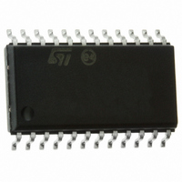
ST72F63BE1M1 STMicroelectronics, ST72F63BE1M1 Datasheet - Page 92

ST72F63BE1M1
Manufacturer Part Number
ST72F63BE1M1
Description
IC MCU 8BIT 4K FLASH 24-SOIC
Manufacturer
STMicroelectronics
Series
ST7r
Datasheet
1.ST72F63BD6U1TR.pdf
(186 pages)
Specifications of ST72F63BE1M1
Core Processor
ST7
Core Size
8-Bit
Speed
8MHz
Connectivity
I²C, SCI, USB
Peripherals
DMA, LVD, POR, PWM, WDT
Number Of I /o
14
Program Memory Size
4KB (4K x 8)
Program Memory Type
FLASH
Ram Size
384 x 8
Voltage - Supply (vcc/vdd)
4 V ~ 5.5 V
Oscillator Type
External
Operating Temperature
0°C ~ 70°C
Package / Case
24-SOIC (7.5mm Width)
Data Converters
A/D 12x8b
Processor Series
ST72F6x
Core
ST7
Data Bus Width
8 bit
Data Ram Size
384 B
Interface Type
I2C, SCI
Maximum Clock Frequency
8 MHz
Number Of Programmable I/os
14
Number Of Timers
1
Maximum Operating Temperature
+ 70 C
Mounting Style
SMD/SMT
Development Tools By Supplier
ST7MDTU3-EPB/US, ST7MDTULS-EVAL, ST72F63B-SK/RAIS, ST7MDTU3-EMU3, STX-RLINK
Minimum Operating Temperature
0 C
For Use With
497-5521 - EVAL BOARD LOW SPEED USB
Lead Free Status / RoHS Status
Lead free / RoHS Compliant
Eeprom Size
-
Lead Free Status / Rohs Status
Details
Available stocks
Company
Part Number
Manufacturer
Quantity
Price
- Current page: 92 of 186
- Download datasheet (3Mb)
On-chip peripherals
92/186
Control register 1 (SCICR1)
Reset value: x000 0000 (x0h)
R8
7
7 R8 Receive data bit 8.
6 T8 Transmit data bit 8.
5 SCID Disabled for low power consumption
4 M Word length.
3 WAKE Wakeup method.
2 PCE Parity control enable.
1 PS Parity selection.
0 PIE Parity interrupt enable.
T8
This bit is used to store the 9th bit of the received word when M=1.
This bit is used to store the 9th bit of the transmitted word when M=1.
When this bit is set the SCI prescalers and outputs are stopped and the end of the
current byte transfer in order to reduce power consumption.This bit is set and
cleared by software.
0: SCI enabled
1: SCI prescaler and outputs disabled
This bit determines the word length. It is set or cleared by software.
0: 1 Start bit, 8 Data bits, 1 Stop bit
1: 1 Start bit, 9 Data bits, 1 Stop bit
Note: The M bit must not be modified during a data transfer (both transmission
This bit determines the SCI wakeup method, it is set or cleared by software.
0: Idle Line
1: Address Mark
This bit selects the hardware parity control (generation and detection). When the
parity control is enabled, the computed parity is inserted at the MSB position (9th
bit if M=1; 8th bit if M=0) and parity is checked on the received data. This bit is set
and cleared by software. Once it is set, PCE is active after the current byte (in
reception and in transmission).
0: Parity control disabled
1: Parity control enabled
This bit selects the odd or even parity when the parity generation/detection is
enabled (PCE bit set). It is set and cleared by software. The parity will be selected
after the current byte.
0: Even parity
1: Odd parity
This bit enables the interrupt capability of the hardware parity control when a parity
error is detected (PE bit set). It is set and cleared by software.
0: Parity error interrupt disabled
1: Parity error interrupt enabled.
and reception).
SCID
Doc ID 7516 Rev 8
M
Read/write
WAKE
PCE
PS
ST7263Bxx
PIE
0
Related parts for ST72F63BE1M1
Image
Part Number
Description
Manufacturer
Datasheet
Request
R

Part Number:
Description:
KIT STARTER LOW COST ST7
Manufacturer:
STMicroelectronics
Datasheet:

Part Number:
Description:
LOW SPEED USB 8-BIT MCU FAMILY WITH FLASH/ROM, UP TO 512 BYTES RAM, 8-BIT ADC, WDG, TIMER, SCI & I�C
Manufacturer:
STMICROELECTRONICS [STMicroelectronics]
Datasheet:

Part Number:
Description:
STMicroelectronics [RIPPLE-CARRY BINARY COUNTER/DIVIDERS]
Manufacturer:
STMicroelectronics
Datasheet:

Part Number:
Description:
STMicroelectronics [LIQUID-CRYSTAL DISPLAY DRIVERS]
Manufacturer:
STMicroelectronics
Datasheet:

Part Number:
Description:
BOARD EVAL FOR MEMS SENSORS
Manufacturer:
STMicroelectronics
Datasheet:

Part Number:
Description:
NPN TRANSISTOR POWER MODULE
Manufacturer:
STMicroelectronics
Datasheet:

Part Number:
Description:
TURBOSWITCH ULTRA-FAST HIGH VOLTAGE DIODE
Manufacturer:
STMicroelectronics
Datasheet:

Part Number:
Description:
Manufacturer:
STMicroelectronics
Datasheet:

Part Number:
Description:
DIODE / SCR MODULE
Manufacturer:
STMicroelectronics
Datasheet:

Part Number:
Description:
DIODE / SCR MODULE
Manufacturer:
STMicroelectronics
Datasheet:

Part Number:
Description:
Search -----> STE16N100
Manufacturer:
STMicroelectronics
Datasheet:

Part Number:
Description:
Search ---> STE53NA50
Manufacturer:
STMicroelectronics
Datasheet:


