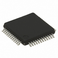
STM8S207C6T6TR STMicroelectronics, STM8S207C6T6TR Datasheet - Page 49

STM8S207C6T6TR
Manufacturer Part Number
STM8S207C6T6TR
Description
MCU 8BIT 32K MEMORY 48LQFP
Manufacturer
STMicroelectronics
Series
STM8Sr
Datasheet
1.STEVAL-MKI030V1.pdf
(105 pages)
Specifications of STM8S207C6T6TR
Mfg Application Notes
STM8S Getting Started
Core Processor
STM8
Core Size
8-Bit
Speed
24MHz
Connectivity
I²C, IrDA, LIN, SPI, UART/USART
Peripherals
Brown-out Detect/Reset, POR, PWM, WDT
Number Of I /o
38
Program Memory Size
32KB (32K x 8)
Program Memory Type
FLASH
Eeprom Size
1K x 8
Ram Size
2K x 8
Voltage - Supply (vcc/vdd)
2.95 V ~ 5.5 V
Data Converters
A/D 10x10b
Oscillator Type
Internal
Operating Temperature
-40°C ~ 85°C
Package / Case
48-LQFP
Processor Series
STM8S20x
Core
STM8
Data Bus Width
8 bit
Data Ram Size
6 KB
Interface Type
CAN,12C,SPI,UART
Maximum Clock Frequency
24 MHz
Number Of Programmable I/os
38
Number Of Timers
2
Operating Supply Voltage
2.95 V to 5.5 V
Maximum Operating Temperature
+ 85 C
Mounting Style
SMD/SMT
3rd Party Development Tools
EWSTM8
Development Tools By Supplier
STICE-SYS001
Minimum Operating Temperature
- 40 C
On-chip Adc
10 bit
For Use With
497-10032 - EVAL KIT MOTOR CONTROL STM8S497-10031 - EVAL KIT TOUCH SENSING STM8S497-10592 - BOARD DAUGHTER FOR STM8S207/8497-10593 - KIT STARTER FOR STM8S207/8 SER497-8506 - BOARD EVAL FOR STM8S
Lead Free Status / RoHS Status
Lead free / RoHS Compliant
Available stocks
Company
Part Number
Manufacturer
Quantity
Price
Company:
Part Number:
STM8S207C6T6TR
Manufacturer:
ST
Quantity:
4 200
Company:
Part Number:
STM8S207C6T6TR
Manufacturer:
STMicroelectronics
Quantity:
10 000
STM8S207xx, STM8S208xx
Table 13.
Option byte no.
OPT0
OPT1
OPT2
Option byte description
ROP[7:0] Memory readout protection (ROP)
UBC[7:0] User boot code area
AFR7Alternate function remapping option 7
AFR6 Alternate function remapping option 6
AFR5 Alternate function remapping option 5
AFR4 Alternate function remapping option 4
AFR3 Alternate function remapping option 3
AFR2 Alternate function remapping option 2
AFR1 Alternate function remapping option 1
AFR0 Alternate function remapping option 0
0xAA: Enable readout protection (write access via SWIM protocol)
Note: Refer to the family reference manual (RM0016) section on
Flash/EEPROM memory readout protection for details.
0x00: no UBC, no write-protection
0x01: Pages 0 to 1 defined as UBC, memory write-protected
0x02: Pages 0 to 3 defined as UBC, memory write-protected
0x03: Pages 0 to 4 defined as UBC, memory write-protected
...
0xFE: Pages 0 to 255 defined as UBC, memory write-protected
0xFF: Reserved
Note: Refer to the family reference manual (RM0016) section on
Flash/EEPROM write protection for more details.
0: Port D4 alternate function = TIM2_CH1
1: Port D4 alternate function = BEEP
0: Port B5 alternate function = AIN5, port B4 alternate function = AIN4
1: Port B5 alternate function = I
I
0: Port B3 alternate function = AIN3, port B2 alternate function = AIN2,
port B1 alternate function = AIN1, port B0 alternate function = AIN0
1: Port B3 alternate function = TIM1_ETR, port B2 alternate function =
TIM1_CH3N, port B1 alternate function = TIM1_CH2N, port B0 alternate
function = TIM1_CH1N
0: Port D7 alternate function = TLI
1: Port D7 alternate function = TIM1_CH4
0: Port D0 alternate function = TIM3_CH2
1: Port D0 alternate function = TIM1_BKIN
0: Port D0 alternate function = TIM3_CH2
1: Port D0 alternate function = CLK_CCO
Note: AFR2 option has priority over AFR3 if both are activated
0: Port A3 alternate function = TIM2_CH3, port D2 alternate function
TIM3_CH1
1: Port A3 alternate function = TIM3_CH1, port D2 alternate function
TIM2_CH3
0: Port D3 alternate function = TIM2_CH2
1: Port D3 alternate function = ADC_ETR
2
C_SCL
Doc ID 14733 Rev 11
Description
2
C_SDA, port B4 alternate function =
Option bytes
49/105


