ST7FLITE39F2M6 STMicroelectronics, ST7FLITE39F2M6 Datasheet - Page 69

ST7FLITE39F2M6
Manufacturer Part Number
ST7FLITE39F2M6
Description
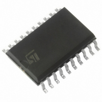
IC MCU 8BIT 8K FLASH 20SOIC
Manufacturer
STMicroelectronics
Series
ST7r
Datasheet
1.ST7FLITE35F2M6TR.pdf
(173 pages)
Specifications of ST7FLITE39F2M6
Core Processor
ST7
Core Size
8-Bit
Speed
16MHz
Connectivity
LINSCI, SPI
Peripherals
LVD, POR, PWM, WDT
Number Of I /o
15
Program Memory Size
8KB (8K x 8)
Program Memory Type
FLASH
Eeprom Size
256 x 8
Ram Size
384 x 8
Voltage - Supply (vcc/vdd)
2.7 V ~ 5.5 V
Data Converters
A/D 7x10b
Oscillator Type
Internal
Operating Temperature
-40°C ~ 85°C
Package / Case
20-SOIC (7.5mm Width)
Processor Series
ST7FLITE3x
Core
ST7
Data Bus Width
8 bit
Data Ram Size
384 B
Interface Type
LINSCI, SPI
Maximum Clock Frequency
8 MHz
Number Of Programmable I/os
15
Number Of Timers
4
Maximum Operating Temperature
+ 85 C
Mounting Style
SMD/SMT
Development Tools By Supplier
ST7FLITE-SK/RAIS, ST7MDT10-DVP3, ST7MDT10-EMU3, STX-RLINK
Minimum Operating Temperature
- 40 C
On-chip Adc
10 bit, 7 Channel
For Use With
497-8406 - BOARD STF20NM50FD/STF7LITE39BF2497-8403 - BOARD DEMO STCC08 AC SW DETECTOR497-6398 - BOARD EVAL ST7FLITE39/STM1403497-5858 - EVAL BOARD PLAYBACK ST7FLITE497-5514 - EVAL BOARD THERMO CONTROL REFRIG497-5049 - KIT STARTER RAISONANCE ST7FLITE
Lead Free Status / RoHS Status
Lead free / RoHS Compliant
Other names
497-5641-5
STFLITE39F2M6
STFLITE39F2M6
Available stocks
Company
Part Number
Manufacturer
Quantity
Price
DUAL 12-BIT AUTORELOAD TIMER 3 (Cont’d)
Bit 4 = BPEN Break Pin Enable.
This bit is read/write by software and cleared by
hardware after Reset.
0: Break pin disabled
1: Break pin enabled
Bit 3:0 = PWM[3:0] Break Pattern.
These bits are read/write by software and cleared
by hardware after a reset. They are used to force
the four PWMx output signals into a stable state
when the Break function is active.
PWMx DUTY CYCLE REGISTER HIGH (DCRxH)
Read / Write
Reset Value: 0000 0000 (00h)
PWMx DUTY CYCLE REGISTER LOW (DCRxL)
Read / Write
Reset Value: 0000 0000 (00h)
Bits 15:12 = Reserved.
Bits 11:0 = DCRx[11:0] PWMx Duty Cycle Value
This 12-bit value is written by software. It defines
the duty cycle of the corresponding PWM output
signal (see
In PWM mode (OEx=1 in the PWMCR register)
the DCR[11:0] bits define the duty cycle of the
PWMx output signal (see
Compare mode, they define the value to be com-
pared with the 12-bit upcounter value.
DCR7 DCR6 DCR5 DCR4 DCR3 DCR2 DCR1 DCR0
15
0
7
0
Figure
0
37).
0
DCR11 DCR10 DCR9 DCR8
Figure
37). In Output
8
0
INPUT CAPTURE REGISTER HIGH (ATICRH)
Read only
Reset Value: 0000 0000 (00h)
INPUT CAPTURE REGISTER LOW (ATICRL)
Read only
Reset Value: 0000 0000 (00h)
Bits 15:12 = Reserved.
Bits 11:0 = ICR[11:0] Input Capture Data.
This is a 12-bit register which is readable by soft-
ware and cleared by hardware after a reset. The
ATICR register contains captured the value of the
12-bit CNTR1 register when a rising or falling edge
occurs on the ATIC or LTIC pin (depending on
ICS). Capture will only be performed when the ICF
flag is cleared.
TIMER CONTROL REGISTER2 (ATCSR2)
Read/Write
Reset Value: 0000 0011 (03h)
Bits 7:6 = Reserved. Forced by hardware to 0.
Bit 5 = ICS Input Capture Shorted
This bit is read/write by software. It allows the AT-
timer CNTR1 to use the LTIC pin for long input
capture.
0 : ATIC for CNTR1 input capture
1 : LTIC for CNTR1 input capture
ICR7
15
0
7
7
0
ICR6
0
0
ICR5
ICS
0
OVFIE2 OVF2
ICR4
0
ICR11 ICR10
ICR3
ENCNT
ICR2
R2
ST7LITE3xF2
TRAN2 TRAN1
ICR9
ICR1
69/173
ICR8
ICR0
8
0
0
1


