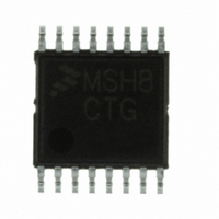
MC9S08SH8CTG Freescale Semiconductor, MC9S08SH8CTG Datasheet - Page 255

MC9S08SH8CTG
Manufacturer Part Number
MC9S08SH8CTG
Description
IC MCU 8BIT 8K FLASH 16-TSSOP
Manufacturer
Freescale Semiconductor
Series
HCS08r
Datasheet
1.MC9S08SH4CTJ.pdf
(338 pages)
Specifications of MC9S08SH8CTG
Core Processor
HCS08
Core Size
8-Bit
Speed
40MHz
Connectivity
I²C, LIN, SCI, SPI
Peripherals
LVD, POR, PWM, WDT
Number Of I /o
13
Program Memory Size
8KB (8K x 8)
Program Memory Type
FLASH
Ram Size
512 x 8
Voltage - Supply (vcc/vdd)
2.7 V ~ 5.5 V
Data Converters
A/D 8x10b
Oscillator Type
Internal
Operating Temperature
-40°C ~ 85°C
Package / Case
16-TSSOP
Cpu Family
HCS08
Device Core Size
8b
Frequency (max)
40MHz
Interface Type
I2C/SCI/SPI
Total Internal Ram Size
512Byte
# I/os (max)
13
Number Of Timers - General Purpose
1
Operating Supply Voltage (typ)
3.3/5V
Operating Supply Voltage (max)
5.5V
Operating Supply Voltage (min)
2.7V
On-chip Adc
8-chx10-bit
Instruction Set Architecture
CISC
Operating Temp Range
-40C to 85C
Operating Temperature Classification
Industrial
Mounting
Surface Mount
Pin Count
16
Package Type
TSSOP
Processor Series
S08SH
Core
HCS08
Data Bus Width
8 bit
Data Ram Size
512 B
Maximum Clock Frequency
40 MHz
Number Of Programmable I/os
13
Number Of Timers
3
Operating Supply Voltage
5.5 V
Maximum Operating Temperature
+ 85 C
Mounting Style
SMD/SMT
3rd Party Development Tools
EWS08
Development Tools By Supplier
DEMO9S08SG32, DEMO9S08SG32AUTO, DEMO9S08SG8, DEMO9S08SG8AUTO, DEMO9S08SH32, DEMO9S08SH8
Minimum Operating Temperature
- 40 C
For Use With
DEMO9S08SH8 - BOARD DEMO FOR MC9S08SH FAM
Lead Free Status / RoHS Status
Lead free / RoHS Compliant
Eeprom Size
-
Lead Free Status / Rohs Status
Compliant
Available stocks
Company
Part Number
Manufacturer
Quantity
Price
Company:
Part Number:
MC9S08SH8CTG
Manufacturer:
FREESCALE
Quantity:
12 000
Part Number:
MC9S08SH8CTG
Manufacturer:
FREESCALE
Quantity:
20 000
Part Number:
MC9S08SH8CTGR
Manufacturer:
FREESCALE
Quantity:
20 000
- Current page: 255 of 338
- Download datasheet (4Mb)
The following sections describe the main counter and each of the timer operating modes (input capture,
output compare, edge-aligned PWM, and center-aligned PWM). Because details of pin operation and
interrupt activity depend upon the operating mode, these topics will be covered in the associated mode
explanation sections.
16.4.1
All timer functions are based on the main 16-bit counter (TPMxCNTH:TPMxCNTL). This section
discusses selection of the clock source, end-of-count overflow, up-counting vs. up/down counting, and
manual counter reset.
16.4.1.1
The 2-bit field, CLKSB:CLKSA, in the timer status and control register (TPMxSC) selects one of three
possible clock sources or OFF (which effectively disables the TPM). See
CLKSB:CLKSA=0:0 so no clock source is selected, and the TPM is in a very low power state. These
control bits may be read or written at any time and disabling the timer (writing 00 to the CLKSB:CLKSA
field) does not affect the values in the counter or other timer registers.
The bus rate clock is the main system bus clock for the MCU. This clock source requires no
synchronization because it is the clock that is used for all internal MCU activities including operation of
the CPU and buses.
In MCUs that have no PLL and FLL or the PLL and FLL are not engaged, the fixed system clock source
is the same as the bus-rate-clock source, and it does not go through a synchronizer. When a PLL or FLL
is present and engaged, a synchronizer is required between the crystal divided-by two clock source and the
timer counter so counter transitions will be properly aligned to bus-clock transitions. A synchronizer will
be used at chip level to synchronize the crystal-related source clock to the bus clock.
The external clock source may be connected to any TPM channel pin. This clock source always has to pass
through a synchronizer to assure that counter transitions are properly aligned to bus clock transitions. The
bus-rate clock drives the synchronizer; therefore, to meet Nyquist criteria even with jitter, the frequency of
the external clock source must not be faster than the bus rate divided-by four. With ideal clocks the external
clock can be as fast as bus clock divided by four.
When the external clock source shares the TPM channel pin, this pin should not be used for other channel
timing functions. For example, it would be ambiguous to configure channel 0 for input capture when the
TPM channel 0 pin was also being used as the timer external clock source. (It is the user’s responsibility
Freescale Semiconductor
Counter
Counter Clock Source
CLKSB:CLKSA
00
01
10
11
Table 16-8. TPM Clock Source Selection
MC9S08SH8 MCU Series Data Sheet, Rev. 3
No clock selected (TPM counter disabled)
TPM Clock Source to Prescaler Input
Fixed system clock
External source
Bus rate clock
Chapter 16 Timer/PWM Module (S08TPMV3)
Table
16-4. After any MCU reset,
255
Related parts for MC9S08SH8CTG
Image
Part Number
Description
Manufacturer
Datasheet
Request
R
Part Number:
Description:
Manufacturer:
Freescale Semiconductor, Inc
Datasheet:
Part Number:
Description:
Manufacturer:
Freescale Semiconductor, Inc
Datasheet:
Part Number:
Description:
Manufacturer:
Freescale Semiconductor, Inc
Datasheet:
Part Number:
Description:
Manufacturer:
Freescale Semiconductor, Inc
Datasheet:
Part Number:
Description:
Manufacturer:
Freescale Semiconductor, Inc
Datasheet:
Part Number:
Description:
Manufacturer:
Freescale Semiconductor, Inc
Datasheet:
Part Number:
Description:
Manufacturer:
Freescale Semiconductor, Inc
Datasheet:
Part Number:
Description:
Manufacturer:
Freescale Semiconductor, Inc
Datasheet:
Part Number:
Description:
Manufacturer:
Freescale Semiconductor, Inc
Datasheet:
Part Number:
Description:
Manufacturer:
Freescale Semiconductor, Inc
Datasheet:
Part Number:
Description:
Manufacturer:
Freescale Semiconductor, Inc
Datasheet:
Part Number:
Description:
Manufacturer:
Freescale Semiconductor, Inc
Datasheet:
Part Number:
Description:
Manufacturer:
Freescale Semiconductor, Inc
Datasheet:
Part Number:
Description:
Manufacturer:
Freescale Semiconductor, Inc
Datasheet:
Part Number:
Description:
Manufacturer:
Freescale Semiconductor, Inc
Datasheet:


