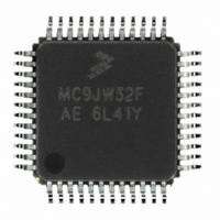
MCHC908JW32FAE Freescale Semiconductor, MCHC908JW32FAE Datasheet - Page 102

MCHC908JW32FAE
Manufacturer Part Number
MCHC908JW32FAE
Description
IC MCU 32K FLASH 8MHZ 48-LQFP
Manufacturer
Freescale Semiconductor
Series
HC08r
Datasheet
1.RD3152MMA7260Q.pdf
(232 pages)
Specifications of MCHC908JW32FAE
Core Processor
HC08
Core Size
8-Bit
Speed
8MHz
Connectivity
SPI, USB
Peripherals
LED, LVD, POR, PWM
Number Of I /o
29
Program Memory Size
32KB (32K x 8)
Program Memory Type
FLASH
Ram Size
1K x 8
Voltage - Supply (vcc/vdd)
3.5 V ~ 5.5 V
Oscillator Type
Internal
Operating Temperature
0°C ~ 70°C
Package / Case
48-LQFP
Controller Family/series
HC08
No. Of I/o's
48
Ram Memory Size
1KB
Cpu Speed
8MHz
No. Of Timers
1
Embedded Interface Type
SPI
Rohs Compliant
Yes
Processor Series
HC08JW
Core
HC08
Data Bus Width
8 bit
Data Ram Size
1 KB
Interface Type
SPI, USB
Number Of Programmable I/os
29
Number Of Timers
2
Maximum Operating Temperature
+ 70 C
Mounting Style
SMD/SMT
Development Tools By Supplier
FSICEBASE, DEMO908GZ60E, M68EML08GZE, KITUSBSPIDGLEVME, KITUSBSPIEVME, KIT33810EKEVME
Minimum Operating Temperature
0 C
Lead Free Status / RoHS Status
Lead free / RoHS Compliant
Eeprom Size
-
Data Converters
-
Lead Free Status / Rohs Status
Details
Available stocks
Company
Part Number
Manufacturer
Quantity
Price
Company:
Part Number:
MCHC908JW32FAE
Manufacturer:
Freescale Semiconductor
Quantity:
10 000
Part Number:
MCHC908JW32FAE
Manufacturer:
FREESCALE
Quantity:
20 000
Monitor Mode (MON)
During monitor mode entry, the MCU waits after the power-on reset for the host to send the eight security
bytes on pin PTA0. If the received bytes match those at locations $FFF6–$FFFD, the host bypasses the
security feature and can read all ROM locations and execute code from ROM. Security remains bypassed
until a power-on reset occurs. If the reset was not a power-on reset, security remains bypassed and
security code entry is not required. (See
Upon power-on reset, if the received bytes of the security code do not match the data at locations
$FFF6–$FFFD, the host fails to bypass the security feature. The MCU remains in monitor mode, but
reading a ROM location returns an invalid value and trying to execute code from ROM causes an illegal
address reset. After receiving the eight security bytes from the host, the MCU transmits a break character,
signifying that it is ready to receive a command.
To determine whether the security code entered is correct, check to see if bit 6 of RAM address $60 is
set. If it is, then the correct security code has been entered and ROM can be accessed.
102
PTA0
NOTES:
RST
V
1 = Echo delay, approximately 2 bit times.
2 = Data return delay, approximately 2 bit times.
4 = Wait 1 bit time before sending next byte.
The MCU does not transmit a break character until after the host sends the
eight security bits.
DD
FROM HOST
FROM MCU
Figure 7-7. Monitor Mode Entry Timing
4096 + 32 CGMXCLK CYCLES
MC68HC908JW32 Data Sheet, Rev. 6
Figure
1
256 BUS CYCLES (MINIMUM)
7-7.)
NOTE
4
1
1
2
4
Freescale Semiconductor
1


