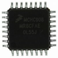
MCHC908MR8CFAE Freescale Semiconductor, MCHC908MR8CFAE Datasheet - Page 312

MCHC908MR8CFAE
Manufacturer Part Number
MCHC908MR8CFAE
Description
IC MCU 8K FLASH 8MHZ PWM 32-LQFP
Manufacturer
Freescale Semiconductor
Series
HC08r
Datasheet
1.MCHC908MR8VFAE.pdf
(372 pages)
Specifications of MCHC908MR8CFAE
Core Processor
HC08
Core Size
8-Bit
Speed
8MHz
Connectivity
SCI
Peripherals
LVD, POR, PWM
Number Of I /o
16
Program Memory Size
8KB (8K x 8)
Program Memory Type
FLASH
Ram Size
256 x 8
Voltage - Supply (vcc/vdd)
4.5 V ~ 5.5 V
Data Converters
A/D 7x10b
Oscillator Type
Internal
Operating Temperature
-40°C ~ 85°C
Package / Case
32-LQFP
Controller Family/series
HC08
No. Of I/o's
16
Ram Memory Size
256Byte
Cpu Speed
8MHz
No. Of Timers
2
Rohs Compliant
Yes
Processor Series
HC08MR
Core
HC08
Data Bus Width
8 bit
Data Ram Size
64 B
Interface Type
SCI, SPI
Maximum Clock Frequency
8 MHz
Number Of Programmable I/os
32
Number Of Timers
4
Operating Supply Voltage
0 V to 5 V
Maximum Operating Temperature
+ 85 C
Mounting Style
SMD/SMT
Development Tools By Supplier
FSICEBASE, M68CBL05CE
Minimum Operating Temperature
- 40 C
On-chip Adc
8 bit, 8 Channel
Lead Free Status / RoHS Status
Lead free / RoHS Compliant
Eeprom Size
-
Lead Free Status / Rohs Status
Details
Available stocks
Company
Part Number
Manufacturer
Quantity
Price
Company:
Part Number:
MCHC908MR8CFAE
Manufacturer:
Freescale Semiconductor
Quantity:
10 000
- Current page: 312 of 372
- Download datasheet (4Mb)
Analog-to-Digital Converter (ADC)
18.2 Introduction
18.3 Features
18.4 Functional Description
Technical Data
312
This section describes the 10-bit analog-to-digital converter (ADC).
For further information regarding analog-to-digital converters on
Freescale microcontrollers, please consult the HC08 ADC Reference
Manual, ADCRM/AD.
Features of the ADC module include:
Depending on the package option, up to seven ADC channels are
available for sampling external sources at pins PTA6/ATD6:PT00/ATD0.
To achieve the best possible accuracy, these pins are implemented as
input-only pins when the analog-to-digital (A/D) feature is enabled. An
analog multiplexer allows the single ADC to select one of the seven ADC
channels as ADC voltage IN (ADCVIN). ADCVIN is converted by the
successive approximation algorithm. When the conversion is completed,
the ADC places the result in the ADC data register (ADRH and ADRL)
and sets a flag or generates an interrupt. See
•
•
•
•
•
•
•
•
•
Four to seven channels with multiplexed input
Linear successive approximation
10-bit resolution, 8-bit accuracy
Single or continuous conversion
Conversion complete flag or conversion complete interrupt
Selectable ADC clock
Left or right justified result.
Left justified sign data mode
High impedance buffered ADC input
Analog-to-Digital Converter (ADC)
Figure
MC68HC908MR8 — Rev 4.1
Freescale Semiconductor
18-1.
Related parts for MCHC908MR8CFAE
Image
Part Number
Description
Manufacturer
Datasheet
Request
R
Part Number:
Description:
Manufacturer:
Freescale Semiconductor, Inc
Datasheet:
Part Number:
Description:
Manufacturer:
Freescale Semiconductor, Inc
Datasheet:
Part Number:
Description:
Manufacturer:
Freescale Semiconductor, Inc
Datasheet:
Part Number:
Description:
Manufacturer:
Freescale Semiconductor, Inc
Datasheet:
Part Number:
Description:
Manufacturer:
Freescale Semiconductor, Inc
Datasheet:
Part Number:
Description:
Manufacturer:
Freescale Semiconductor, Inc
Datasheet:
Part Number:
Description:
Manufacturer:
Freescale Semiconductor, Inc
Datasheet:
Part Number:
Description:
Manufacturer:
Freescale Semiconductor, Inc
Datasheet:
Part Number:
Description:
Manufacturer:
Freescale Semiconductor, Inc
Datasheet:
Part Number:
Description:
Manufacturer:
Freescale Semiconductor, Inc
Datasheet:
Part Number:
Description:
Manufacturer:
Freescale Semiconductor, Inc
Datasheet:
Part Number:
Description:
Manufacturer:
Freescale Semiconductor, Inc
Datasheet:
Part Number:
Description:
Manufacturer:
Freescale Semiconductor, Inc
Datasheet:
Part Number:
Description:
Manufacturer:
Freescale Semiconductor, Inc
Datasheet:
Part Number:
Description:
Manufacturer:
Freescale Semiconductor, Inc
Datasheet:


