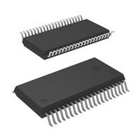
M38504E6FP#U0 Renesas Electronics America, M38504E6FP#U0 Datasheet - Page 20

M38504E6FP#U0
Manufacturer Part Number
M38504E6FP#U0
Description
MCU 4.0/5.5V 24K PB-FREE 42-SSOP
Manufacturer
Renesas Electronics America
Series
740/38000r
Datasheet
1.M38504E6FPU0.pdf
(103 pages)
Specifications of M38504E6FP#U0
Core Processor
740
Core Size
8-Bit
Speed
8MHz
Connectivity
SIO, UART/USART
Peripherals
PWM, WDT
Number Of I /o
32
Program Memory Size
24KB (24K x 8)
Program Memory Type
OTP
Ram Size
640 x 8
Voltage - Supply (vcc/vdd)
1.8 V ~ 5.5 V
Data Converters
A/D 5x10b
Oscillator Type
Internal
Operating Temperature
-20°C ~ 85°C
Package / Case
42-SSOP
Lead Free Status / RoHS Status
Lead free / RoHS Compliant
Eeprom Size
-
Available stocks
Company
Part Number
Manufacturer
Quantity
Price
3850 Group (Spec.A)
I/O PORTS
The I/O ports have direction registers which determine the input/
output direction of each individual pin. Each bit in a direction
register corresponds to one pin, and each pin can be set to be
input port or output port.
When “0” is written to the bit corresponding to a pin, that pin
becomes an input pin. When “1” is written to that bit, that pin
becomes an output pin.
If data is read from a pin which is set to output, the value of the
port output latch is read, not the value of the pin itself. Pins set to
input are floating. If a pin set to input is written to, only the port
output latch is written to and the pin remains floating.
Table 9 I/O port function (spec. A)
Note: When bits 5 to 7 of Ports P3 and P4 are read out, the contents are undefined.
Rev.3.01
P0
P0
P0
P0
P0
P1
P2
P2
P2
P2
P2
P2
P2
P2
P3
P3
P4
P4
P4
P4
P4
0
1
2
3
4
0
0
1
2
3
4
5
6
7
0
4
0
1
2
3
4
/S
/S
/S
/S
/AN
–P1
/X
/X
/RxD
/TxD
/S
/CNTR
/AN
/AN
/CNTR
/INT
/INT
/INT
/INT
IN2
OUT2
CLK2
RDY2
COUT
CIN
CLK1
Pin
5
0
4
7
0
1
2
3
–P0
–
/S
/PWM
0
1
2003.06.20
CMP2
/S
7
AN
RDY1
8
Port P0
Port P1
Port P2
Port P3
Port P4
(Note)
Name
page 18 of 98
Input/Output
Input/output,
individual
bits
CMOS compatible
input level
N-channel open-drain
output
CMOS compatible
input level
CMOS 3-state output
CMOS compatible
input level
CMOS 3-state output
I/O Structure
By setting the port P0, P1, P2 pull-up control register (address
0012
the port P4 pull-up control register (address 0014
control pull-up with a program. However, the contents of these
registers do not affect ports programmed as the output ports.
Serial I/O2 function I/O
A-D conversion input
Serial I/O1 function I/O
A-D conversion input
External interrupt input
External interrupt input
PWM output
Sub-clock generating
circuit
Serial I/O1 function I/O
Timer X function I/O
Timer Y function I/O
External interrupt input
S
CMP2
16
Non-Port Function
), the port P3 pull-up control register (address 0013
output
CPU mode register
Serial I/O2 control register
A-D control register
A-D input selection register
Serial I/O1 control register
Timer XY mode register
Serial I/O1 control register
Timer XY mode register
Interrupt edge selection
register
Serial I/O2 control register
Interrupt edge selection
register
PWM control register
A-D control register
A-D input selection register
Interrupt edge selection
register
Related SFRs
16
), ports can
Ref.No.
16
(13)
(10)
(11)
(12)
(13)
(14)
(15)
(16)
(17)
(1)
(2)
(3)
(4)
(5)
(6)
(7)
(8)
(9)
), or


