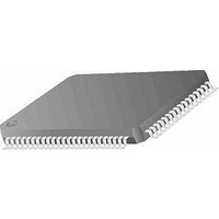
MC68HC11K0CFUE4 Freescale Semiconductor, MC68HC11K0CFUE4 Datasheet - Page 98

MC68HC11K0CFUE4
Manufacturer Part Number
MC68HC11K0CFUE4
Description
MCU 8-BIT 768 RAM 4MHZ 80-QFP
Manufacturer
Freescale Semiconductor
Series
HC11r
Specifications of MC68HC11K0CFUE4
Core Processor
HC11
Core Size
8-Bit
Speed
4MHz
Connectivity
SCI, SPI
Peripherals
POR, PWM, WDT
Number Of I /o
37
Program Memory Type
ROMless
Ram Size
768 x 8
Voltage - Supply (vcc/vdd)
4.5 V ~ 5.5 V
Data Converters
A/D 8x8b
Oscillator Type
Internal
Operating Temperature
-40°C ~ 85°C
Package / Case
80-QFP
Data Bus Width
8 bit
Data Ram Size
768 B
Interface Type
SCI, SPI
Maximum Clock Frequency
4 MHz
Number Of Programmable I/os
37
Number Of Timers
8
Maximum Operating Temperature
+ 85 C
Mounting Style
SMD/SMT
Minimum Operating Temperature
- 40 C
On-chip Adc
8 bit, 8 Channel
Lead Free Status / RoHS Status
Lead free / RoHS Compliant
Eeprom Size
-
Program Memory Size
-
Lead Free Status / Rohs Status
Details
Available stocks
Company
Part Number
Manufacturer
Quantity
Price
Company:
Part Number:
MC68HC11K0CFUE4
Manufacturer:
Freescale Semiconductor
Quantity:
10 000
- Current page: 98 of 290
- Download datasheet (4Mb)
Operating Modes and On-Chip Memory
4.8.2.1 EEPROM Programming
Technical Data
98
The procedures for both writing and erasing involve these five steps:
The following examples demonstrate programming a single EEPROM
byte, erasing the entire EEPROM, erasing a row (16 bytes), and erasing
a single byte.
On entry, accumulator A contains the data to be written and X points to
the address to be programmed.
1. Set the EELAT bit in PPROG. If erasing, also set the ERASE bit
2. Write data to the appropriate EEPROM address. If erasing, any
3. Set the EEPGM bit in PPROG, keeping EELAT set. If erasing,
4. Delay for 10 ms.
5. Clear the PPROG register to turn off the high voltage and
Freescale Semiconductor, Inc.
EEPROG
For More Information On This Product,
and the appropriate BYTE and ROW bits.
data will work. To erase a row, write to any location in the row. To
erase the entire EEPROM, write to any location in the array. This
step is done before applying the programming voltage because
setting the EEPGM bit inhibits writes to EEPROM addresses.
also set the ERASE bit and the appropriate BYTE and ROW bits.
reconfigure the EEPROM address and data buses for normal
operation.
Operating Modes and On-Chip Memory
Go to: www.freescale.com
LDAB
STAB
STAA
LDAB
STAB
JSR
CLR
#$02
$003B
$0,X
#$03
$002B
DLY10
$003B
Set EELAT bit to enable EEPROM
latches.
Store data to EPROM address
Set EPGM bit with ELAT=1
to enable EEPROM programming voltage
Delay 10 ms
Turn off programming voltage and set
to READ mode
M68HC11K Family
MOTOROLA
Related parts for MC68HC11K0CFUE4
Image
Part Number
Description
Manufacturer
Datasheet
Request
R

Part Number:
Description:
MC68HC11 EEPROM Programming from a Personal Computer
Manufacturer:
Motorola / Freescale Semiconductor
Part Number:
Description:
Manufacturer:
Freescale Semiconductor, Inc
Datasheet:
Part Number:
Description:
Manufacturer:
Freescale Semiconductor, Inc
Datasheet:
Part Number:
Description:
Manufacturer:
Freescale Semiconductor, Inc
Datasheet:
Part Number:
Description:
Manufacturer:
Freescale Semiconductor, Inc
Datasheet:
Part Number:
Description:
Manufacturer:
Freescale Semiconductor, Inc
Datasheet:
Part Number:
Description:
Manufacturer:
Freescale Semiconductor, Inc
Datasheet:
Part Number:
Description:
Manufacturer:
Freescale Semiconductor, Inc
Datasheet:
Part Number:
Description:
Manufacturer:
Freescale Semiconductor, Inc
Datasheet:
Part Number:
Description:
Manufacturer:
Freescale Semiconductor, Inc
Datasheet:
Part Number:
Description:
Manufacturer:
Freescale Semiconductor, Inc
Datasheet:
Part Number:
Description:
Manufacturer:
Freescale Semiconductor, Inc
Datasheet:
Part Number:
Description:
Manufacturer:
Freescale Semiconductor, Inc
Datasheet:
Part Number:
Description:
Manufacturer:
Freescale Semiconductor, Inc
Datasheet:
Part Number:
Description:
Manufacturer:
Freescale Semiconductor, Inc
Datasheet:


