M30876FJAGP#U3 Renesas Electronics America, M30876FJAGP#U3 Datasheet - Page 89
M30876FJAGP#U3
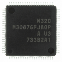
Manufacturer Part Number
M30876FJAGP#U3
Description
IC M32C/87 MCU FLASH 100LQFP
Manufacturer
Renesas Electronics America
Series
M16C™ M32C/80r
Datasheet
1.M3087BFLGPU3.pdf
(629 pages)
Specifications of M30876FJAGP#U3
Core Processor
M32C/80
Core Size
16/32-Bit
Speed
32MHz
Connectivity
CAN, EBI/EMI, I²C, IEBus, IrDA, SIO, UART/USART
Peripherals
DMA, POR, PWM, WDT
Number Of I /o
85
Program Memory Size
512KB (512K x 8)
Program Memory Type
FLASH
Ram Size
31K x 8
Voltage - Supply (vcc/vdd)
3 V ~ 5.5 V
Data Converters
A/D 26x10b; D/A 2x8b
Oscillator Type
Internal
Operating Temperature
-40°C ~ 85°C
Package / Case
100-LQFP
For Use With
R0K330879S001BE - KIT DEV RSK M32C/87R0K330879S000BE - KIT DEV RSK M32C/87
Lead Free Status / RoHS Status
Lead free / RoHS Compliant
Eeprom Size
-
Available stocks
Company
Part Number
Manufacturer
Quantity
Price


M32C/87 Group (M32C/87, M32C/87A, M32C/87B)
REJ09B0180-0151 Rev.1.51 Jul 31, 2008
Page 65 of 587
Table 8.3
NOTES:
PM05 and
PM04 bits
setting
Data bus width
P0_0 to P0_7
P1_0 to P1_7
P2_0 to P2_7
P3_0 to P3_7
P4_0 to P4_3
P4_4 to P4_6
P4_7
P5_0 to P5_2
P5_3
P5_4
P5_5
P5_6
P5_7
Processor
1. Do not set bits PM05 and PM04 in the PM0 register to 11b (access all CS areas using multiplexed bus) in
2. These pins are used as address bus when selecting separate bus.
3. Bits PM15 and PM14 in the PM1 register determine which pin is used to output the ALE signal.
4. The PM02 bit in the PM0 register selects either combination, “RD, WRL, WRH” or “RD, BHE, WR”.
5. P5_6 outputs undefined value when bits PM15 and PM14 are set to 00b (no ALE). In this case, it cannot be
6. Bits PM11 and PM10 in the PM1 register determine whether these pins are used as chip-select outputs or
7. Use bits CM01 and CM00 in the CM0 register, bits PM15 and PM14 in the PM1 register, and the PM07 bit in
Mode
microprocessor mode since the MCU starts up with the separate bus after reset. When bits PM05 and PM04
are set to 11b in memory expansion mode, the accessible space is 64-Kbyte per each chip-select output.
used as an I/O port.
address bus.
the PM0 register to select among CLKOUT, BCLK, and ALE function.
(1)
Processor Mode and Pin Function
Single-chip
I/O port
I/O port/
CLKOUT
I/O port
Mode
00b
(Multiplexed bus not used)
Access all
external
spaces with
8-bit data
bus
Data bus (D0 to D7)
I/O port
Address bus (A0 to A7)
Address bus (A8 to A15)
Address Bus (A16 to A19)
CS or address bus (A20 to A22) (Refer to 8.2 Bus Control for details)
CS or address bus (A23) (Refer to 8.2 Bus Control for details)
RD, WRL, WRH outputs or RD, BHE, WR outputs
(Refer to 8.2 Bus Control for details)
CLKOUT/BCLK/ALE
HLDA/ALE
HOLD
ALE
RDY
(3)(5)
Memory Expansion Mode/Microprocessor Mode
(3)
Access any
external
spaces with
16-bit data
bus
Data bus
(D8 to D15)
(7)
01b (Access CS2 area
using multiplexed bus)
10b (Access CS1 area
using multiplexed bus)
Access all
external
spaces with
8-bit data
bus
I/O port
Address bus/data bus (A0/D0 to A7/D7)
(4)
Access any
external
spaces with
16-bit data
bus
Data bus
(D8 to D15)
Address bus/
data bus
(A8/D8 to
A15/D15)
(2)
Memory Expansion Mode
11b
(Access all CS areas using
multiplexed bus)
Access all
external
spaces with
8-bit data
bus
I/O port
Address bus
(A8 to A15)
I/O port
(6)
(2)
(6)
Access any
external
spaces with
16-bit data
bus
Address bus/
data bus
(A8/D8 to
A15/D15)
(2)
8. Bus
Related parts for M30876FJAGP#U3
Image
Part Number
Description
Manufacturer
Datasheet
Request
R

Part Number:
Description:
KIT STARTER FOR M16C/29
Manufacturer:
Renesas Electronics America
Datasheet:

Part Number:
Description:
KIT STARTER FOR R8C/2D
Manufacturer:
Renesas Electronics America
Datasheet:

Part Number:
Description:
R0K33062P STARTER KIT
Manufacturer:
Renesas Electronics America
Datasheet:

Part Number:
Description:
KIT STARTER FOR R8C/23 E8A
Manufacturer:
Renesas Electronics America
Datasheet:

Part Number:
Description:
KIT STARTER FOR R8C/25
Manufacturer:
Renesas Electronics America
Datasheet:

Part Number:
Description:
KIT STARTER H8S2456 SHARPE DSPLY
Manufacturer:
Renesas Electronics America
Datasheet:

Part Number:
Description:
KIT STARTER FOR R8C38C
Manufacturer:
Renesas Electronics America
Datasheet:

Part Number:
Description:
KIT STARTER FOR R8C35C
Manufacturer:
Renesas Electronics America
Datasheet:

Part Number:
Description:
KIT STARTER FOR R8CL3AC+LCD APPS
Manufacturer:
Renesas Electronics America
Datasheet:
Part Number:
Description:
KIT STARTER FOR RX610
Manufacturer:
Renesas Electronics America
Datasheet:

Part Number:
Description:
KIT STARTER FOR R32C/118
Manufacturer:
Renesas Electronics America
Datasheet:

Part Number:
Description:
KIT DEV RSK-R8C/26-29
Manufacturer:
Renesas Electronics America
Datasheet:

Part Number:
Description:
KIT STARTER FOR SH7124
Manufacturer:
Renesas Electronics America
Datasheet:

Part Number:
Description:
KIT STARTER FOR H8SX/1622
Manufacturer:
Renesas Electronics America
Datasheet:

Part Number:
Description:
KIT DEV FOR SH7203
Manufacturer:
Renesas Electronics America
Datasheet: