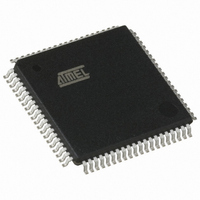
AT80C51SND1C-ROTIL Atmel, AT80C51SND1C-ROTIL Datasheet - Page 10

AT80C51SND1C-ROTIL
Manufacturer Part Number
AT80C51SND1C-ROTIL
Description
IC MCU FLASH MP3 DECODER 80-TQFP
Manufacturer
Atmel
Series
80Cr
Datasheet
1.AT80C51SND1C-ROTIL.pdf
(213 pages)
Specifications of AT80C51SND1C-ROTIL
Core Processor
8051
Core Size
8-Bit
Speed
40MHz
Connectivity
I²C, IDE/ATAPI, MMC, SPI, UART/USART, USB
Peripherals
Audio, I²S, MP3, PCM, POR, WDT
Number Of I /o
44
Program Memory Type
ROMless
Ram Size
2.25K x 8
Voltage - Supply (vcc/vdd)
2.7 V ~ 3.3 V
Data Converters
A/D 2x10b
Oscillator Type
Internal
Operating Temperature
-40°C ~ 85°C
Package / Case
80-TQFP, 80-VQFP
Lead Free Status / RoHS Status
Contains lead / RoHS non-compliant
Eeprom Size
-
Program Memory Size
-
Other names
AT80C51SND1CROTIL
Available stocks
Company
Part Number
Manufacturer
Quantity
Price
- Current page: 10 of 213
- Download datasheet (3Mb)
10
AT8xC51SND1C
Table 11. Keypad Interface Signal Description
Table 12. External Access Signal Description
Notes:
Table 13. System Signal Description
1. For ROM/Flash Dice product versions: pad EA must be connected to VCC.
2. For ROMless Dice product versions: pad EA must be connected to VSS.
Signal
KIN3:0
Signal
EA
Signal
AD7:0
Name
Name
PSEN
Name
A15:8
ALE
RST
TST
ISP
WR
RD
(1)(2)
Type
Type
Type
I/O
I/O
I/O
I/O
O
O
O
I
I
I
I
Description
Keypad Input Lines
Holding one of these pins high or low for 24 oscillator periods triggers a
keypad interrupt.
Description
Address Lines
Upper address lines for the external bus.
Multiplexed higher address and data lines for the IDE interface.
Address/Data Lines
Multiplexed lower address and data lines for the external memory or the
IDE interface.
Address Latch Enable Output
ALE signals the start of an external bus cycle and indicates that valid
address information is available on lines A7:0. An external latch is used
to demultiplex the address from address/data bus.
Program Store Enable Output (AT80C51SND1C Only)
This signal is active low during external code fetch or external code
read (MOVC instruction).
ISP Enable Input (AT89C51SND1C Only)
This signal must be held to GND through a pull-down resistor at the
falling reset to force execution of the internal bootloader.
Read Signal
Read signal asserted during external data memory read operation.
Write Signal
Write signal asserted during external data memory write operation.
External Access Enable (Dice Only)
EA must be externally held low to enable the device to fetch code from
external program memory locations 0000h to FFFFh.
Description
Reset Input
Holding this pin high for 64 oscillator periods while the oscillator is
running resets the device. The Port pins are driven to their reset
conditions when a voltage lower than V
oscillator is running.
This pin has an internal pull-down resistor which allows the device to be
reset by connecting a capacitor between this pin and V
Asserting RST when the chip is in Idle mode or Power-Down mode
returns the chip to normal operation.
Test Input
Test mode entry signal. This pin must be set to V
IL
is applied, whether or not the
DD
.
DD
.
4109L–8051–02/08
Alternate
Alternate
Alternate
Function
Function
Function
P1.3:0
P2.7:0
P0.7:0
P3.7
P3.6
-
-
-
-
-
-
Related parts for AT80C51SND1C-ROTIL
Image
Part Number
Description
Manufacturer
Datasheet
Request
R

Part Number:
Description:
DEV KIT FOR AVR/AVR32
Manufacturer:
Atmel
Datasheet:

Part Number:
Description:
INTERVAL AND WIPE/WASH WIPER CONTROL IC WITH DELAY
Manufacturer:
ATMEL Corporation
Datasheet:

Part Number:
Description:
Low-Voltage Voice-Switched IC for Hands-Free Operation
Manufacturer:
ATMEL Corporation
Datasheet:

Part Number:
Description:
MONOLITHIC INTEGRATED FEATUREPHONE CIRCUIT
Manufacturer:
ATMEL Corporation
Datasheet:

Part Number:
Description:
AM-FM Receiver IC U4255BM-M
Manufacturer:
ATMEL Corporation
Datasheet:

Part Number:
Description:
Monolithic Integrated Feature Phone Circuit
Manufacturer:
ATMEL Corporation
Datasheet:

Part Number:
Description:
Multistandard Video-IF and Quasi Parallel Sound Processing
Manufacturer:
ATMEL Corporation
Datasheet:

Part Number:
Description:
High-performance EE PLD
Manufacturer:
ATMEL Corporation
Datasheet:

Part Number:
Description:
8-bit Flash Microcontroller
Manufacturer:
ATMEL Corporation
Datasheet:

Part Number:
Description:
2-Wire Serial EEPROM
Manufacturer:
ATMEL Corporation
Datasheet:


