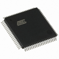
AT80C51SND1C-ROTIL Atmel, AT80C51SND1C-ROTIL Datasheet - Page 28

AT80C51SND1C-ROTIL
Manufacturer Part Number
AT80C51SND1C-ROTIL
Description
IC MCU FLASH MP3 DECODER 80-TQFP
Manufacturer
Atmel
Series
80Cr
Datasheet
1.AT80C51SND1C-ROTIL.pdf
(213 pages)
Specifications of AT80C51SND1C-ROTIL
Core Processor
8051
Core Size
8-Bit
Speed
40MHz
Connectivity
I²C, IDE/ATAPI, MMC, SPI, UART/USART, USB
Peripherals
Audio, I²S, MP3, PCM, POR, WDT
Number Of I /o
44
Program Memory Type
ROMless
Ram Size
2.25K x 8
Voltage - Supply (vcc/vdd)
2.7 V ~ 3.3 V
Data Converters
A/D 2x10b
Oscillator Type
Internal
Operating Temperature
-40°C ~ 85°C
Package / Case
80-TQFP, 80-VQFP
Lead Free Status / RoHS Status
Contains lead / RoHS non-compliant
Eeprom Size
-
Program Memory Size
-
Other names
AT80C51SND1CROTIL
Available stocks
Company
Part Number
Manufacturer
Quantity
Price
- Current page: 28 of 213
- Download datasheet (3Mb)
7.2.2
7.2.3
28
AT8xC51SND1C
Page Access Mode
External Bus Cycles
Figure 3 shows the structure of the external address bus. P0 carries address A7:0 while P2 car-
ries address A15:8. Data D7:0 is multiplexed with A7:0 on P0. Table 28 describes the external
memory interface signals.
Figure 3. External Data Memory Interface Structure
Table 28. External Data Memory Interface Signals
The AT8xC51SND1C implement a feature called Page Access that disables the output of DPH
on P2 when executing MOVX @DPTR instruction. Page Access is enable by setting the DPH-
DIS bit in AUXR register.
Page Access is useful when application uses both ERAM and 256 Bytes of XRAM. In this case,
software modifies intensively EXTRAM bit to select access to ERAM or XRAM and must save it
if used in interrupt service routine. Page Access allows external access above 00FFh address
without generating DPH on P2. Thus ERAM is accessed using MOVX @Ri or MOVX @DPTR
with DPTR < 0100h, < 0200h, < 0400h or < 0800h depending on the XRS1:0 bits value. Then
XRAM is accessed using MOVX @DPTR with DPTR ≥ 0800h regardless of XRS1:0 bits value
while keeping P2 for general I/O usage.
This section describes the bus cycles the AT8xC51SND1C executes to read (see Figure 4), and
write data (see Figure 5) in the external data memory.
External memory cycle takes 6 CPU clock periods. This is equivalent to 12 oscillator clock period
Signal
Name
AD7:0
A15:8
ALE
WR
RD
Type
I/O
O
O
O
O
AT8xC51SND1C
Description
Address Lines
Upper address lines for the external bus.
Address/Data Lines
Multiplexed lower address lines and data for the external memory.
Address Latch Enable
ALE signals indicates that valid address information are available on lines
AD7:0.
Read
Read signal output to external data memory.
Write
Write signal output to external memory.
ALE
WR
RD
P2
P0
AD7:0
A15:8
Latch
A7:0
A15:8
A7:0
D7:0
OE
WR
PERIPHERAL
RAM
4109L–8051–02/08
Alternate
Function
P2.7:0
P0.7:0
P3.7
P3.6
-
Related parts for AT80C51SND1C-ROTIL
Image
Part Number
Description
Manufacturer
Datasheet
Request
R

Part Number:
Description:
DEV KIT FOR AVR/AVR32
Manufacturer:
Atmel
Datasheet:

Part Number:
Description:
INTERVAL AND WIPE/WASH WIPER CONTROL IC WITH DELAY
Manufacturer:
ATMEL Corporation
Datasheet:

Part Number:
Description:
Low-Voltage Voice-Switched IC for Hands-Free Operation
Manufacturer:
ATMEL Corporation
Datasheet:

Part Number:
Description:
MONOLITHIC INTEGRATED FEATUREPHONE CIRCUIT
Manufacturer:
ATMEL Corporation
Datasheet:

Part Number:
Description:
AM-FM Receiver IC U4255BM-M
Manufacturer:
ATMEL Corporation
Datasheet:

Part Number:
Description:
Monolithic Integrated Feature Phone Circuit
Manufacturer:
ATMEL Corporation
Datasheet:

Part Number:
Description:
Multistandard Video-IF and Quasi Parallel Sound Processing
Manufacturer:
ATMEL Corporation
Datasheet:

Part Number:
Description:
High-performance EE PLD
Manufacturer:
ATMEL Corporation
Datasheet:

Part Number:
Description:
8-bit Flash Microcontroller
Manufacturer:
ATMEL Corporation
Datasheet:

Part Number:
Description:
2-Wire Serial EEPROM
Manufacturer:
ATMEL Corporation
Datasheet:


