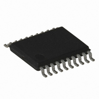
ATTINY167-15XD Atmel, ATTINY167-15XD Datasheet - Page 204

ATTINY167-15XD
Manufacturer Part Number
ATTINY167-15XD
Description
MCU AVR 16K FLASH 15MHZ 20-TSSOP
Manufacturer
Atmel
Series
AVR® ATtinyr
Datasheet
1.ATTINY167-15MD.pdf
(283 pages)
Specifications of ATTINY167-15XD
Core Processor
AVR
Core Size
8-Bit
Speed
16MHz
Connectivity
I²C, LIN, SPI, UART/USART, USI
Peripherals
Brown-out Detect/Reset, POR, PWM, Temp Sensor, WDT
Number Of I /o
16
Program Memory Size
16KB (8K x 16)
Program Memory Type
FLASH
Eeprom Size
512 x 8
Ram Size
512 x 8
Voltage - Supply (vcc/vdd)
2.7 V ~ 5.5 V
Data Converters
A/D 11x10b
Oscillator Type
Internal
Operating Temperature
-40°C ~ 150°C
Package / Case
20-TSSOP
Processor Series
ATTINY1x
Core
AVR8
Data Bus Width
8 bit
Data Ram Size
512 B
Maximum Clock Frequency
16 MHz
Maximum Operating Temperature
+ 85 C
Mounting Style
SMD/SMT
3rd Party Development Tools
EWAVR, EWAVR-BL
Development Tools By Supplier
ATAVRDRAGON, ATSTK500, ATSTK600, ATAVRISP2, ATAVRONEKIT
Minimum Operating Temperature
- 40 C
For Use With
ATSTK600-SOIC - STK600 SOCKET/ADAPTER FOR SOIC
Lead Free Status / RoHS Status
Lead free / RoHS Compliant
- Current page: 204 of 283
- Download datasheet (5Mb)
17.10 Internal Voltage Reference Output
204
ATtiny87/ATtiny167
The following code example allows to read Signature Row data:
The internal voltage reference is output on XREF pin as described in
turned on
of an external filter capacitor (5 - 10 nF) on XREF pin may be necessary. XREF current load
must be from 1 µA to 100 µA with VCC from 2.7V to 5.5V for XREF = 1.1V and with VCC from
4.5V to 5.5V for XREF = 2.56V.
XREF pin can be coupled to an analog input of the ADC
Table 17-3.
Notes:
XREFEN
.equ TS_GAIN = 0x0007
.equ TS_OFFSET = 0x0005
LDI R30,LOW(TS_GAIN)
LDI R31,HIGH (TS_GAIN)
RCALL Read_signature_row
MOV R17,R16 ; Save R16 result
LDI R30,LOW(TS_OFFSET)
LDI R31,HIGH (TS_OFFSET)
RCALL Read_signature_row
; R16 holds TS_OFFSET and R17 holds TS_GAIN
Read_signature_row:
IN R16,SPMCSR ; Wait for SPMEN ready
SBRC R16,SPMEN ; Exit loop here when SPMCSR is free
RJMP Read_signature_row
LDI R16,((1<<SIGRD)|(1<<SPMEN)) ; We need to set SIGRD and SPMEN
together
OUT SPMCSR,R16 ; and execute the LPM within 3 cycles
LPM R16,Z
RET
1
1
0
(1)
(1)
1.
2.
3. In these configurations, the pin pull-up must be turned off and the pin digital output must be
4. Vcc in range 4.5 - 5.5V.
(See “Voltage Reference Enable Signals and Start-up Time” on page
(1)
See ”Bit 1 – XREFEN: Internal Voltage Reference Output Enable” on page 210.
See ”Bit 7:6 – REFS1:REFS0: Voltage Reference Selection Bits” on page 205.
set in Hi-Z.
Internal Voltage Reference Output
REFS1
x
0
1
(2)
REFS0
1
1
x
(2)
Voltage Reference Output (I
Hi-Z, the pin can be used as AREF input or other alternate
functions.
XREF = 1.1V
XREF = 2.56V
(3)
(3)(4)
(See ”Pin Configuration” on page
load
Table 17-3
100 µA)
7728G–AVR–06/10
53.). Addition
if the ADC is
5.).
Related parts for ATTINY167-15XD
Image
Part Number
Description
Manufacturer
Datasheet
Request
R

Part Number:
Description:
Manufacturer:
Atmel Corporation
Datasheet:

Part Number:
Description:
Manufacturer:
Atmel Corporation
Datasheet:

Part Number:
Description:
MCU AVR 16K FLASH 15MHZ 32-QFN
Manufacturer:
Atmel
Datasheet:

Part Number:
Description:
IC MCU AVR 16K FLASH 20TSSOP
Manufacturer:
Atmel
Datasheet:

Part Number:
Description:
MCU AVR 16K FLASH 15MHZ 32-QFN
Manufacturer:
Atmel
Datasheet:

Part Number:
Description:
MCU AVR 16K FLASH 15MHZ 20-SOIC
Manufacturer:
Atmel
Datasheet:

Part Number:
Description:
MCU AVR 16K FLASH 15MHZ 20-TSSOP
Manufacturer:
Atmel
Datasheet:

Part Number:
Description:
IC MCU AVR 16K FLASH 20SOIC
Manufacturer:
Atmel
Datasheet:


