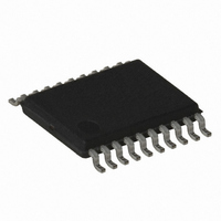
ATTINY167-15XD Atmel, ATTINY167-15XD Datasheet - Page 209

ATTINY167-15XD
Manufacturer Part Number
ATTINY167-15XD
Description
MCU AVR 16K FLASH 15MHZ 20-TSSOP
Manufacturer
Atmel
Series
AVR® ATtinyr
Datasheet
1.ATTINY167-15MD.pdf
(283 pages)
Specifications of ATTINY167-15XD
Core Processor
AVR
Core Size
8-Bit
Speed
16MHz
Connectivity
I²C, LIN, SPI, UART/USART, USI
Peripherals
Brown-out Detect/Reset, POR, PWM, Temp Sensor, WDT
Number Of I /o
16
Program Memory Size
16KB (8K x 16)
Program Memory Type
FLASH
Eeprom Size
512 x 8
Ram Size
512 x 8
Voltage - Supply (vcc/vdd)
2.7 V ~ 5.5 V
Data Converters
A/D 11x10b
Oscillator Type
Internal
Operating Temperature
-40°C ~ 150°C
Package / Case
20-TSSOP
Processor Series
ATTINY1x
Core
AVR8
Data Bus Width
8 bit
Data Ram Size
512 B
Maximum Clock Frequency
16 MHz
Maximum Operating Temperature
+ 85 C
Mounting Style
SMD/SMT
3rd Party Development Tools
EWAVR, EWAVR-BL
Development Tools By Supplier
ATAVRDRAGON, ATSTK500, ATSTK600, ATAVRISP2, ATAVRONEKIT
Minimum Operating Temperature
- 40 C
For Use With
ATSTK600-SOIC - STK600 SOCKET/ADAPTER FOR SOIC
Lead Free Status / RoHS Status
Lead free / RoHS Compliant
- Current page: 209 of 283
- Download datasheet (5Mb)
17.11.4
17.11.5
7728G–AVR–06/10
ADCSRB – ADC Control and Status Register B
DIDR0 – Digital Input Disable Register 0
• Bit 7– BIN: Bipolar Input Mode
The gain stage is working in the unipolar mode as default, but the bipolar mode can be
selected by writing the BIN bit in the ADCSRB register. In the unipolar mode only one-sided
conversions are supported and the voltage on the positive input must always be larger than
the voltage on the negative input. Otherwise the result is saturated to the voltage reference. In
the bipolar mode two-sided conversions are supported and the result is represented in the
two’s complement form. In the unipolar mode the resolution is 10 bits and the bipolar mode the
resolution is 9 bits + 1 sign bit.
• Bit 3 – Res: Reserved Bit
This bit is reserved for future use. For compatibility with future devices it must be written to
zero when ADCSRB register is written.
• Bits 2:0 – ADTS2:0: ADC Auto Trigger Source
If ADATE in ADCSRA register is written to one, the value of these bits selects which source
will trigger an ADC conversion. If ADATE is cleared, the ADTS2:0 settings will have no effect.
A conversion will be triggered by the rising edge of the selected Interrupt Flag. Note that
switching from a trigger source that is cleared to a trigger source that is set, will generate a
positive edge on the trigger signal. If ADEN in ADCSRA register is set, this will start a conver-
sion. Switching to Free Running mode (ADTS[2:0]=0) will not cause a trigger event, even if the
ADC Interrupt Flag is set.
Table 17-7.
Bit
Read/Write
Initial Value
Bit
Read/Write
Initial Value
ADTS2
0
0
0
0
1
1
1
1
ADC7D /
ADC Auto Trigger Source Selections
AIN1D
R/W
R/W
BIN
7
0
7
0
ADTS1
ADC6D /
0
0
1
1
0
0
1
1
AIN0D
ACME
R/W
R/W
6
0
6
0
ADC5D
ACIR1
R/W
R/W
5
0
5
0
ADTS0
0
1
0
1
0
1
0
1
ADC4D
ACIR0
R/W
R/W
4
0
4
0
Trigger Source
Free Running mode
Analog Comparator
External Interrupt Request 0
Timer/Counter1 Compare Match A
Timer/Counter1 Overflow
Timer/Counter1 Compare Match B
Timer/Counter1 Capture Event
Watchdog Interrupt Request
ADC3D
R/W
R
3
0
3
–
0
ATtiny87/ATtiny167
ADC2D
ADTS2
R/W
R/W
2
0
2
0
ADC1D
ADTS1
R/W
R/W
1
0
1
0
ADC0D
ADTS0
R/W
R/W
0
0
0
0
ADCSRB
DIDR0
209
Related parts for ATTINY167-15XD
Image
Part Number
Description
Manufacturer
Datasheet
Request
R

Part Number:
Description:
Manufacturer:
Atmel Corporation
Datasheet:

Part Number:
Description:
Manufacturer:
Atmel Corporation
Datasheet:

Part Number:
Description:
MCU AVR 16K FLASH 15MHZ 32-QFN
Manufacturer:
Atmel
Datasheet:

Part Number:
Description:
IC MCU AVR 16K FLASH 20TSSOP
Manufacturer:
Atmel
Datasheet:

Part Number:
Description:
MCU AVR 16K FLASH 15MHZ 32-QFN
Manufacturer:
Atmel
Datasheet:

Part Number:
Description:
MCU AVR 16K FLASH 15MHZ 20-SOIC
Manufacturer:
Atmel
Datasheet:

Part Number:
Description:
MCU AVR 16K FLASH 15MHZ 20-TSSOP
Manufacturer:
Atmel
Datasheet:

Part Number:
Description:
IC MCU AVR 16K FLASH 20SOIC
Manufacturer:
Atmel
Datasheet:


