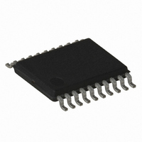
ATTINY167-15XD Atmel, ATTINY167-15XD Datasheet - Page 23

ATTINY167-15XD
Manufacturer Part Number
ATTINY167-15XD
Description
MCU AVR 16K FLASH 15MHZ 20-TSSOP
Manufacturer
Atmel
Series
AVR® ATtinyr
Datasheet
1.ATTINY167-15MD.pdf
(283 pages)
Specifications of ATTINY167-15XD
Core Processor
AVR
Core Size
8-Bit
Speed
16MHz
Connectivity
I²C, LIN, SPI, UART/USART, USI
Peripherals
Brown-out Detect/Reset, POR, PWM, Temp Sensor, WDT
Number Of I /o
16
Program Memory Size
16KB (8K x 16)
Program Memory Type
FLASH
Eeprom Size
512 x 8
Ram Size
512 x 8
Voltage - Supply (vcc/vdd)
2.7 V ~ 5.5 V
Data Converters
A/D 11x10b
Oscillator Type
Internal
Operating Temperature
-40°C ~ 150°C
Package / Case
20-TSSOP
Processor Series
ATTINY1x
Core
AVR8
Data Bus Width
8 bit
Data Ram Size
512 B
Maximum Clock Frequency
16 MHz
Maximum Operating Temperature
+ 85 C
Mounting Style
SMD/SMT
3rd Party Development Tools
EWAVR, EWAVR-BL
Development Tools By Supplier
ATAVRDRAGON, ATSTK500, ATSTK600, ATAVRISP2, ATAVRONEKIT
Minimum Operating Temperature
- 40 C
For Use With
ATSTK600-SOIC - STK600 SOCKET/ADAPTER FOR SOIC
Lead Free Status / RoHS Status
Lead free / RoHS Compliant
- Current page: 23 of 283
- Download datasheet (5Mb)
3.5.4
3.5.5
3.5.6
7728G–AVR–06/10
General Purpose I/O Register 2 – GPIOR2
General Purpose I/O Register 1 – GPIOR1
General Purpose I/O Register 0 – GPIOR0
• Bit 3 – EERIE: EEPROM Ready Interrupt Enable
Writing EERIE to one enables the EEPROM Ready Interrupt if the I-bit in SREG is set. Writing
EERIE to zero disables the interrupt. The EEPROM Ready Interrupt generates a constant
interrupt when Non-volatile memory is ready for programming.
• Bit 2 – EEMPE: EEPROM Master Program Enable
The EEMPE bit determines whether writing EEPE to one will have effect or not.
When EEMPE is set, setting EEPE within four clock cycles will program the EEPROM at the
selected address. If EEMPE is zero, setting EEPE will have no effect. When EEMPE has been
written to one by software, hardware clears the bit to zero after four clock cycles.
• Bit 1 – EEPE: EEPROM Program Enable
The EEPROM Program Enable Signal EEPE is the programming enable signal to the
EEPROM. When EEPE is written, the EEPROM will be programmed according to the EEPMn
bits setting. The EEMPE bit must be written to one before a logical one is written to EEPE, oth-
erwise no EEPROM write takes place. When the write access time has elapsed, the EEPE bit
is cleared by hardware. When EEPE has been set, the CPU is halted for two cycles before the
next instruction is executed.
• Bit 0 – EERE: EEPROM Read Enable
The EEPROM Read Enable Signal – EERE – is the read strobe to the EEPROM. When the
correct address is set up in the EEAR Register, the EERE bit must be written to one to trigger
the EEPROM read. The EEPROM read access takes one instruction, and the requested data
is available immediately. When the EEPROM is read, the CPU is halted for four cycles before
the next instruction is executed. The user should poll the EEPE bit before starting the read
operation. If a write operation is in progress, it is neither possible to read the EEPROM, nor to
change the EEAR Register.
Bit
Read/Write
Initial Value
Bit
Read/Write
Initial Value
Bit
Read/Write
Initial Value
GPIOR27
GPIOR17
GPIOR07
R/W
R/W
R/W
7
0
7
0
7
0
GPIOR26
GPIOR16
GPIOR06
R/W
R/W
R/W
6
0
6
0
6
0
GPIOR25
GPIOR15
GPIOR05
R/W
R/W
R/W
5
0
5
0
5
0
GPIOR24
GPIOR14
GPIOR04
R/W
R/W
R/W
4
0
4
0
4
0
GPIOR23
GPIOR13
GPIOR03
R/W
R/W
R/W
3
0
3
0
3
0
ATtiny87/ATtiny167
GPIOR12
GPIOR02
GPIOR22
R/W
R/W
R/W
2
0
2
0
2
0
GPIOR11
GPIOR01
GPIOR21
R/W
R/W
R/W
1
0
1
0
1
0
GPIOR10
GPIOR00
GPIOR20
R/W
R/W
R/W
0
0
0
0
0
0
GPIOR1
GPIOR0
GPIOR2
23
Related parts for ATTINY167-15XD
Image
Part Number
Description
Manufacturer
Datasheet
Request
R

Part Number:
Description:
Manufacturer:
Atmel Corporation
Datasheet:

Part Number:
Description:
Manufacturer:
Atmel Corporation
Datasheet:

Part Number:
Description:
MCU AVR 16K FLASH 15MHZ 32-QFN
Manufacturer:
Atmel
Datasheet:

Part Number:
Description:
IC MCU AVR 16K FLASH 20TSSOP
Manufacturer:
Atmel
Datasheet:

Part Number:
Description:
MCU AVR 16K FLASH 15MHZ 32-QFN
Manufacturer:
Atmel
Datasheet:

Part Number:
Description:
MCU AVR 16K FLASH 15MHZ 20-SOIC
Manufacturer:
Atmel
Datasheet:

Part Number:
Description:
MCU AVR 16K FLASH 15MHZ 20-TSSOP
Manufacturer:
Atmel
Datasheet:

Part Number:
Description:
IC MCU AVR 16K FLASH 20SOIC
Manufacturer:
Atmel
Datasheet:


