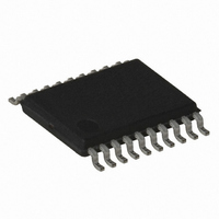
ATTINY167-15XD Atmel, ATTINY167-15XD Datasheet - Page 77

ATTINY167-15XD
Manufacturer Part Number
ATTINY167-15XD
Description
MCU AVR 16K FLASH 15MHZ 20-TSSOP
Manufacturer
Atmel
Series
AVR® ATtinyr
Datasheet
1.ATTINY167-15MD.pdf
(283 pages)
Specifications of ATTINY167-15XD
Core Processor
AVR
Core Size
8-Bit
Speed
16MHz
Connectivity
I²C, LIN, SPI, UART/USART, USI
Peripherals
Brown-out Detect/Reset, POR, PWM, Temp Sensor, WDT
Number Of I /o
16
Program Memory Size
16KB (8K x 16)
Program Memory Type
FLASH
Eeprom Size
512 x 8
Ram Size
512 x 8
Voltage - Supply (vcc/vdd)
2.7 V ~ 5.5 V
Data Converters
A/D 11x10b
Oscillator Type
Internal
Operating Temperature
-40°C ~ 150°C
Package / Case
20-TSSOP
Processor Series
ATTINY1x
Core
AVR8
Data Bus Width
8 bit
Data Ram Size
512 B
Maximum Clock Frequency
16 MHz
Maximum Operating Temperature
+ 85 C
Mounting Style
SMD/SMT
3rd Party Development Tools
EWAVR, EWAVR-BL
Development Tools By Supplier
ATAVRDRAGON, ATSTK500, ATSTK600, ATAVRISP2, ATAVRONEKIT
Minimum Operating Temperature
- 40 C
For Use With
ATSTK600-SOIC - STK600 SOCKET/ADAPTER FOR SOIC
Lead Free Status / RoHS Status
Lead free / RoHS Compliant
- Current page: 77 of 283
- Download datasheet (5Mb)
7728G–AVR–06/10
The alternate pin configuration is as follows:
• PCINT7/ADC7/AIN1/XREF/AREF – Port A, Bit7
• PCINT6/ADC6/AIN0/SS – Port A, Bit6
• PCINT5/ADC5/T1/USCK/SCL/SCK – Port A, Bit5
• PCINT4/ADC4/ICP1/DI/SDA/MOSI – Port A, Bit 4
PCINT7: Pin Change Interrupt, source 7.
ADC7: Analog to Digital Converter, channel 7.
AIN1: Analog Comparator Positive Input. This pin is directly connected to the positive input
XREF: Internal Voltage Reference Output. The internal voltage reference 2.56V or 1.1V is
AREF: External Voltage Reference Input for ADC. The pin port pull-up and digital output
PCINT6: Pin Change Interrupt, source 6.
ADC6: Analog to Digital Converter, channel 6.
AIN0: Analog Comparator Negative Input. This pin is directly connected to the negative input
SS: SPI Slave Select Input. When the SPI is enabled as a slave, this pin is configured as an
PCINT5: Pin Change Interrupt, source 5.
ADC5: Analog to Digital Converter, channel 5.
T1: Timer/Counter1 Clock Input.
USCK: Three-wire Mode USI Clock Input.
SCL: Two-wire Mode USI Clock Input.
SCK: SPI Master Clock output, Slave Clock input pin. When the SPI is enabled as a slave,
PCINT4: Pin Change Interrupt, source 4.
ADC4: Analog to Digital Converter, channel 4.
ICP1: Timer/Counter1 Input Capture Trigger. The PA3 pin can act as an Input Capture pin for
DI: Three-wire Mode USI Data Input. USI Three-wire mode does not override normal port
SDA: Two-wire Mode Serial Interface (USI) Data Input / Output.
MOSI: SPI Master Output / Slave Input. When the SPI is enabled as a Slave, this pin is con-
of the Analog Comparator.
output when XREFEN is set and if either 2.56V or 1.1V is used as reference for ADC
conversion. When XREF output is enabled, the pin port pull-up and digital output
driver are turned off.
driver are disabled when the pin is used as an external voltage reference input for
ADC or as when the pin is only used to connect a bypass capacitor for the voltage ref-
erence of the ADC.
of the Analog Comparator.
input regardless of the setting of DDA6. As a slave, the SPI is activated when this pin
is driven low. When the SPI is enabled as a master, the data direction of this pin is
controlled by DDA6. When the pin is forced to be an input, the pull-up can still be con-
trolled by the PORTA6 bit.
this pin is configured as an input regardless of the setting of DDA5. When the SPI is
enabled as a master, the data direction of this pin is controlled by DDA5. When the pin
is forced to be an input, the pull-up can still be controlled by the PORTA5 bit.
Timer/Counter1.
functions, so pin must be configure as an input for DI function.
figured as an input regardless of the setting of DDA3. When the SPI is enabled as a
ATtiny87/ATtiny167
77
Related parts for ATTINY167-15XD
Image
Part Number
Description
Manufacturer
Datasheet
Request
R

Part Number:
Description:
Manufacturer:
Atmel Corporation
Datasheet:

Part Number:
Description:
Manufacturer:
Atmel Corporation
Datasheet:

Part Number:
Description:
MCU AVR 16K FLASH 15MHZ 32-QFN
Manufacturer:
Atmel
Datasheet:

Part Number:
Description:
IC MCU AVR 16K FLASH 20TSSOP
Manufacturer:
Atmel
Datasheet:

Part Number:
Description:
MCU AVR 16K FLASH 15MHZ 32-QFN
Manufacturer:
Atmel
Datasheet:

Part Number:
Description:
MCU AVR 16K FLASH 15MHZ 20-SOIC
Manufacturer:
Atmel
Datasheet:

Part Number:
Description:
MCU AVR 16K FLASH 15MHZ 20-TSSOP
Manufacturer:
Atmel
Datasheet:

Part Number:
Description:
IC MCU AVR 16K FLASH 20SOIC
Manufacturer:
Atmel
Datasheet:


