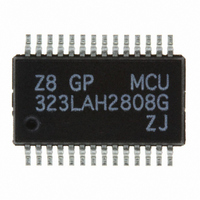
ZGP323LAH2808G Zilog, ZGP323LAH2808G Datasheet - Page 53

ZGP323LAH2808G
Manufacturer Part Number
ZGP323LAH2808G
Description
IC Z8 GP MCU 8K OTP 28SSOP
Manufacturer
Zilog
Series
Z8® GP™r
Specifications of ZGP323LAH2808G
Core Processor
Z8
Core Size
8-Bit
Speed
8MHz
Peripherals
HLVD, POR, WDT
Number Of I /o
24
Program Memory Size
8KB (8K x 8)
Program Memory Type
OTP
Ram Size
237 x 8
Voltage - Supply (vcc/vdd)
2 V ~ 3.6 V
Oscillator Type
Internal
Operating Temperature
-40°C ~ 125°C
Package / Case
28-SSOP
Lead Free Status / RoHS Status
Lead free / RoHS Compliant
Eeprom Size
-
Data Converters
-
Connectivity
-
Other names
269-4409
ZGP323LAH2808G
ZGP323LAH2808G
- Current page: 53 of 107
- Download datasheet (3Mb)
PS023709-0208
cycle. Bit 6 controls whether a low level or a high level at the XOR-gate input (see
Figure 33
after recovery. Bits D2, D3, and D4 of the SMR register specify the source of the Stop
Mode Recovery signal. Bits D0 determines if SCLK/TCLK are divided by 16 or not. The
SMR is located in Bank F of the Expanded Register Group at address
SCLK/TCLK Divide-by-16 Select (D0)
D0 of the SMR controls a divide-by-16 prescaler of SCLK/TCLK (see
control selectively reduces device power consumption during normal processor execution
D7
* Default after Power-On Reset or Watchdog Reset.
* * Set after Stop Mode Recovery.
* * * At the XOR gate input.
* * * * Default setting after reset. Must be 1 if using a crystal or resonator clock source.
SMR(0F)0BH
D6
on page 52) is required from the recovery source. Bit 5 controls the reset delay
D5
Figure 31. Stop Mode Recovery Register
D4
D3
D2
D1
D0
SCLK/TCLK Divide-by-16
0 OFF * *
1 ON
Reserved (Must be 0)
Stop Mode Recovery Source
000 POR Only *
001 Reserved
010 P31
011 P32
100 P33
101 P27
110 P2 NOR 0-3
111 P2 NOR 0-7
Stop Delay
0 OFF
1 ON * * * *
Stop Recovery Level * * *
0 Low *
1 High
Stop Flag
0 POR *
1 Stop Recovery * *
Product Specification
Functional Description
0BH
Figure
.
32). This
ZGP323L
49
Related parts for ZGP323LAH2808G
Image
Part Number
Description
Manufacturer
Datasheet
Request
R

Part Number:
Description:
PLATFORM DEV ICE Z8 GP ZGP323
Manufacturer:
Zilog
Datasheet:

Part Number:
Description:
Communication Controllers, ZILOG INTELLIGENT PERIPHERAL CONTROLLER (ZIP)
Manufacturer:
Zilog, Inc.
Datasheet:

Part Number:
Description:
KIT DEV FOR Z8 ENCORE 16K TO 64K
Manufacturer:
Zilog
Datasheet:

Part Number:
Description:
KIT DEV Z8 ENCORE XP 28-PIN
Manufacturer:
Zilog
Datasheet:

Part Number:
Description:
DEV KIT FOR Z8 ENCORE 8K/4K
Manufacturer:
Zilog
Datasheet:

Part Number:
Description:
KIT DEV Z8 ENCORE XP 28-PIN
Manufacturer:
Zilog
Datasheet:

Part Number:
Description:
DEV KIT FOR Z8 ENCORE 4K TO 8K
Manufacturer:
Zilog
Datasheet:

Part Number:
Description:
CMOS Z8 microcontroller. ROM 16 Kbytes, RAM 256 bytes, speed 16 MHz, 32 lines I/O, 3.0V to 5.5V
Manufacturer:
Zilog, Inc.
Datasheet:

Part Number:
Description:
Low-cost microcontroller. 512 bytes ROM, 61 bytes RAM, 8 MHz
Manufacturer:
Zilog, Inc.
Datasheet:

Part Number:
Description:
Z8 4K OTP Microcontroller
Manufacturer:
Zilog, Inc.
Datasheet:

Part Number:
Description:
CMOS SUPER8 ROMLESS MCU
Manufacturer:
Zilog, Inc.
Datasheet:

Part Number:
Description:
SL1866 CMOSZ8 OTP Microcontroller
Manufacturer:
Zilog, Inc.
Datasheet:

Part Number:
Description:
SL1866 CMOSZ8 OTP Microcontroller
Manufacturer:
Zilog, Inc.
Datasheet:

Part Number:
Description:
OTP (KB) = 1, RAM = 125, Speed = 12, I/O = 14, 8-bit Timers = 2, Comm Interfaces Other Features = Por, LV Protect, Voltage = 4.5-5.5V
Manufacturer:
Zilog, Inc.
Datasheet:


