AD624BDZ Analog Devices Inc, AD624BDZ Datasheet

IC AMP INST 25MHZ PREC LN 16CDIP

AD624BDZ

Manufacturer Part Number
AD624BDZ
Description
IC AMP INST 25MHZ PREC LN 16CDIP
Manufacturer
Analog Devices Inc
Datasheet

Specifications of AD624BDZ

Amplifier Type
Instrumentation
Number Of Circuits
1
Slew Rate
5 V/µs
Gain Bandwidth Product
25MHz
-3db Bandwidth
1MHz
Current - Input Bias
25nA
Voltage - Input Offset
75µV
Current - Supply
3.5mA
Voltage - Supply, Single/dual (±)
±6 V ~ 18 V
Operating Temperature
-25°C ~ 85°C
Mounting Type
Through Hole
Package / Case
16-CDIP (0.300", 7.62mm)
No. Of Amplifiers
1
Input Offset Voltage
75µV
Gain Db Min
1dB
Bandwidth
25MHz
Amplifier Output
Single Ended
Cmrr
120dB
Supply Voltage Range
± 6V To ± 18V
Rohs Compliant
Yes
Lead Free Status / RoHS Status
Lead free / RoHS Compliant
Output Type
-
Current - Output / Channel
-

Available stocks

Company
Part Number
Manufacturer
Quantity
Price
Part Number:
AD624BDZ
Manufacturer:
ADI
Quantity:
651
Part Number:
AD624BDZ
Manufacturer:
AD
Quantity:
780
Part Number:
AD624BDZ
Manufacturer:
ADI
Quantity:
485
Part Number:
AD624BDZ
Manufacturer:
ADI/亚德诺
Quantity:
20 000
a
PRODUCT DESCRIPTION
The AD624 is a high precision, low noise, instrumentation
amplifier designed primarily for use with low level transducers,
including load cells, strain gauges and pressure transducers. An
outstanding combination of low noise, high gain accuracy, low
gain temperature coefficient and high linearity make the AD624
ideal for use in high resolution data acquisition systems.
The AD624C has an input offset voltage drift of less than
0.25 µV/°C, output offset voltage drift of less than 10 µV/°C,
CMRR above 80 dB at unity gain (130 dB at G = 500) and a
maximum nonlinearity of 0.001% at G = 1. In addition to these
outstanding dc specifications, the AD624 exhibits superior ac
performance as well. A 25 MHz gain bandwidth product, 5 V/µs
slew rate and 15 µs settling time permit the use of the AD624 in
high speed data acquisition applications.
The AD624 does not need any external components for pre-
trimmed gains of 1, 100, 200, 500 and 1000. Additional gains
such as 250 and 333 can be programmed within one percent
accuracy with external jumpers. A single external resistor can
also be used to set the 624’s gain to any value in the range of 1
to 10,000.
PRODUCT HIGHLIGHTS
1. The AD624 offers outstanding noise performance. Input
2. The AD624 is a functionally complete instrumentation am-
3. The offset voltage, offset voltage drift, gain accuracy and gain
4. The AD624 provides totally independent input and output
5. A sense terminal is provided to enable the user to minimize
–INPUT
G = 100
G = 200
G = 500
+INPUT
noise is typically less than 4 nV/√Hz at 1 kHz.
plifier. Pin programmable gains of 1, 100, 200, 500 and 1000
are provided on the chip. Other gains are achieved through
the use of a single external resistor.
temperature coefficients are guaranteed for all pretrimmed
gains.
offset nulling terminals for high precision applications.
This minimizes the effect of offset voltage in gain ranging
applications.
the errors induced through long leads. A reference terminal is
also provided to permit level shifting at the output.
RG
RG
1
2
Instrumentation Amplifier
124
80.2
225.3
FUNCTIONAL BLOCK DIAGRAM
50
50
4445.7
V
B
20k
20k
10k
10k
AD624
Precision
AD624
10k
10k
SENSE
OUTPUT
REF

Related parts for AD624BDZ

AD624BDZ Summary of contents

Page 1

PRODUCT DESCRIPTION The AD624 is a high precision, low noise, instrumentation amplifier designed primarily for use with low level transducers, including load cells, strain gauges and pressure transducers. An outstanding combination of low noise, high gain accuracy, low gain ...

Page 2

AD624–SPECIFICATIONS Model AD624A Min GAIN Gain Equation (External Resistor Gain  Programming) 40, 000   Gain Range (Pin Programmable 1000 Gain Error 100 G = 200, 500 Nonlinearity ...

Page 3

Model AD624A Min REFERENCE INPUT ± 10 Voltage Range Gain to Output TEMPERATURE RANGE Specified Performance –25 Storage –65 POWER SUPPLY Power Supply Range 6 Quiescent Current NOTES the maximum differential input ...

Page 4

AD624–Typical Characteristics SUPPLY VOLTAGE – V 8.0 6.0 4.0 2 SUPPLY VOLTAGE – ...

Page 5

G = 500 –120 G = 100 –100 –80 –60 –40 – 100 1k 10k 100k 1M 10M FREQUENCY – Hz 160 –V = –15V dc+ S 140 1V p-p SINEWAVE G = ...

Page 6

AD624 – 0.1% 1% 0.01% – – OUTPUT STEP – – –8 0.01 – SETTLING TIME – s – ...

Page 7

INPUT 100k 20V p 0.1% THEORY OF OPERATION The AD624 is a monolithic instrumentation amplifier based on a modification of the classic three-op-amp instrumentation amplifier. Monolithic construction and laser-wafer-trimming allow the tight matching and tracking of circuit components ...

Page 8

AD624 directly proportional to gain i.e., input offset as measured at the output 100 is 100 times greater than Output offset is independent of gain. At low gains, output offset drift is dominant, ...

Page 9

NOISE The AD624 is designed to provide noise performance near the theoretical noise floor. This is an extremely important design criteria as the front end noise of an instrumentation amplifier is the ultimate limitation on the resolution of the data ...

Page 10

AD624 GROUNDING Many data-acquisition components have two or more ground pins which are not connected together within the device. These grounds must be tied together at one point, usually at the sys- tem power supply ground. Ideally, a single solid ...

Page 11

INPUT OFFSET 4 TRIM 20k R1 5 10k 10k 6 – AD624 + 35V K1 – ANALOG THERMOSEN DM2C COMMON 4.5V COIL D1 – ...

Page 12

AD624 50 +INPUT (–INPUT 100 225.3 4445 200 V B 124 G = 500 80.2 20k 20k 50 –INPUT (+INPUT DAC A DB0 DATA INPUTS DB7 CS AD7528 WR DAC ...

Page 13

WEIGH SCALE Figure 44 shows an example of how an AD624 can be used to condition the differential output voltage from a load cell. The 10% reference voltage adjustment range is required to accom- modate the 10% transducer sensitivity tolerance. ...

Page 14

AD624 ERROR BUDGET ANALYSIS To illustrate how instrumentation amplifier specifications are applied, we will now examine a typical case where an AD624 is required to amplify the output of an unbalanced transducer. Figure 47 shows a differential transducer, unbalanced by ...

Page 15

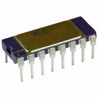
OUTLINE DIMENSIONS Dimensions shown in inches and (mm). Side-Brazed Solder Lid Ceramic DIP (D-16) 0.005 (0.13) MIN 0.080 (2.03) MAX 16 9 0.310 (7.87) 0.220 (5.59 PIN 1 0.060 (1.52) 0.840 (21.34) MAX 0.015 (0.38) 0.200 (5.08) MAX ...

Page 16

...

Related keywords