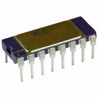
AD624BDZ Analog Devices Inc, AD624BDZ Datasheet - Page 14

AD624BDZ
Manufacturer Part Number
AD624BDZ
Description
IC AMP INST 25MHZ PREC LN 16CDIP
Manufacturer
Analog Devices Inc
Datasheet
1.AD624ADZ.pdf
(16 pages)
Specifications of AD624BDZ
Amplifier Type
Instrumentation
Number Of Circuits
1
Slew Rate
5 V/µs
Gain Bandwidth Product
25MHz
-3db Bandwidth
1MHz
Current - Input Bias
25nA
Voltage - Input Offset
75µV
Current - Supply
3.5mA
Voltage - Supply, Single/dual (±)
±6 V ~ 18 V
Operating Temperature
-25°C ~ 85°C
Mounting Type
Through Hole
Package / Case
16-CDIP (0.300", 7.62mm)
No. Of Amplifiers
1
Input Offset Voltage
75µV
Gain Db Min
1dB
Bandwidth
25MHz
Amplifier Output
Single Ended
Cmrr
120dB
Supply Voltage Range
± 6V To ± 18V
Rohs Compliant
Yes
Lead Free Status / RoHS Status
Lead free / RoHS Compliant
Output Type
-
Current - Output / Channel
-
Available stocks
Company
Part Number
Manufacturer
Quantity
Price
Part Number:
AD624BDZ
Manufacturer:
ADI/亚德诺
Quantity:
20 000
AD624
ERROR BUDGET ANALYSIS
To illustrate how instrumentation amplifier specifications are
applied, we will now examine a typical case where an AD624 is
required to amplify the output of an unbalanced transducer.
Figure 47 shows a differential transducer, unbalanced by ≈5 Ω,
supplying a 0 to 20 mV signal to an AD624C. The output of the
IA feeds a 14-bit A to D converter with a 0 to 2 volt input volt-
age range. The operating temperature range is –25°C to +85°C.
Therefore, the largest change in temperature ∆T within the
operating range is from ambient to +85°C (85°C – 25°C =
60°C.)
In many applications, differential linearity and resolution are of
prime importance. This would be so in cases where the absolute
value of a variable is less important than changes in value. In
these applications, only the irreducible errors (20 ppm =
0.002%) are significant. Furthermore, if a system has an intelli-
gent processor monitoring the A to D output, the addition of an
autogain/autozero cycle will remove all reducible errors and may
eliminate the requirement for initial calibration. This will also
reduce errors to 0.002%.
Error Source
Gain Error
Gain Instability
Gain Nonlinearity
Input Offset Voltage
Input Offset Voltage Drift
Output Offset Voltage
Output Offset Voltage Drift
Bias Current–Source
Offset Current–Source
Offset Current–Source
Offset Current–Source
Common-Mode Rejection
Noise, RTI
NOTE
1
For a comprehensive study of instrumentation amplifier design
and applications, refer to the Instrumentation Amplifier Application
Guide, available free from Analog Devices.
Output offset voltage and output offset voltage drift are given as RTI figures.
Imbalance Error
Imbalance Error
Resistance Error
Resistance–Drift
5 V dc
(0.1 Hz–10 Hz)
1
1
AD624C
Specifications
± 0.1%
10 ppm
± 0.001%
± 25 µV, RTI
± 0.25 µV/°C
± 2.0 mV
± 10 µV/°C
± 15 nA
± 10 nA
± 10 nA
± 100 pA/°C
115 dB
0.22 µV p-p
Table II. Error Budget Analysis of AD624CD in Bridge Application
Calculation
± 0.1% = 1000 ppm
(10 ppm/°C) (60°C) = 600 ppm
± 0.001% = 10 ppm
± 25 µV/20 mV = ± 1250 ppm
(± 0.25 µV/°C) (60°C)= 15 µV
± 2.0 mV/20 mV = 1000 ppm
(± 10 µV/°C) (60°C) = 600 µV
(± 15 nA)(5 Ω ) = 0.075 µV
(± 10 nA)(5 Ω) = 0.050 µV
(10 nA) (175 Ω) = 1.75 µV
(100 pA/°C) (175 Ω) (60°C) = 1 µV
115 dB = 1.8 ppm × 5 V = 9 µV
0.22 µV p-p/20 mV = 10 ppm
15 µV/20 mV = 750 ppm
600 µV/20 mV = 300 ppm
0.075 µV/20mV = 3.75 ppm
0.050 µV/20 mV = 2.5 ppm
1.75 µV/20 mV = 87.5 ppm
1 µV/20 mV = 50 ppm
9 µV/20 mV = 444 ppm
Total Error
350
350
+10V
350
350
Effect on
Absolute
Accuracy
at T
1000 ppm
_
–
1250 ppm
–
1000 ppm
–
3.75 ppm
2.5 ppm
87.5 ppm
–
450 ppm
_
3793.75 ppm
A
G = 100
= +25 C
RG
RG
2
1
Effect on
Absolute
Accuracy
at T
1000 ppm
600 ppm
–
1250 ppm
750 ppm
1000 ppm
300 ppm
3.75 ppm
2.5 ppm
87.5 ppm
50 ppm
450 ppm
–
5493.75 ppm
+V
AD624C
–V
S
A
S
= +85 C Resolution
10k
Effect
on
–
–
10 ppm
–
–
–
–
–
–
–
–
–
10 ppm
20 ppm
0 TO 2V
14-BIT
ADC
F.S.


