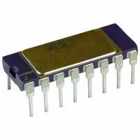
AD624BDZ Analog Devices Inc, AD624BDZ Datasheet - Page 10

AD624BDZ
Manufacturer Part Number
AD624BDZ
Description
IC AMP INST 25MHZ PREC LN 16CDIP
Manufacturer
Analog Devices Inc
Datasheet
1.AD624ADZ.pdf
(16 pages)
Specifications of AD624BDZ
Amplifier Type
Instrumentation
Number Of Circuits
1
Slew Rate
5 V/µs
Gain Bandwidth Product
25MHz
-3db Bandwidth
1MHz
Current - Input Bias
25nA
Voltage - Input Offset
75µV
Current - Supply
3.5mA
Voltage - Supply, Single/dual (±)
±6 V ~ 18 V
Operating Temperature
-25°C ~ 85°C
Mounting Type
Through Hole
Package / Case
16-CDIP (0.300", 7.62mm)
No. Of Amplifiers
1
Input Offset Voltage
75µV
Gain Db Min
1dB
Bandwidth
25MHz
Amplifier Output
Single Ended
Cmrr
120dB
Supply Voltage Range
± 6V To ± 18V
Rohs Compliant
Yes
Lead Free Status / RoHS Status
Lead free / RoHS Compliant
Output Type
-
Current - Output / Channel
-
Available stocks
Company
Part Number
Manufacturer
Quantity
Price
Part Number:
AD624BDZ
Manufacturer:
ADI/亚德诺
Quantity:
20 000
AD624
GROUNDING
Many data-acquisition components have two or more ground
pins which are not connected together within the device. These
grounds must be tied together at one point, usually at the sys-
tem power supply ground. Ideally, a single solid ground would
be desirable. However, since current flows through the ground
wires and etch stripes of the circuit cards, and since these paths
have resistance and inductance, hundreds of millivolts can be
generated between the system ground point and the data acqui-
sition components. Separate ground returns should be provided
to minimize the current flow in the path from the most sensitive
points to the system ground point. In this way supply currents
and logic-gate return currents are not summed into the same
return path as analog signals where they would cause measure-
ment errors (see Figure 34).
Since the output voltage is developed with respect to the poten-
tial on the reference terminal an instrumentation amplifier can
solve many grounding problems.
SENSE TERMINAL
The sense terminal is the feedback point for the instrument
amplifier’s output amplifier. Normally it is connected to the
instrument amplifier output. If heavy load currents are to be
drawn through long leads, voltage drops due to current flowing
through lead resistance can cause errors. The sense terminal can
be wired to the instrument amplifier at the load thus putting the
IxR drops “inside the loop” and virtually eliminating this error
source.
Typically, IC instrumentation amplifiers are rated for a full
± 10 volt output swing into 2 kΩ. In some applications, how-
ever, the need exists to drive more current into heavier loads.
Figure 35 shows how a current booster may be connected
REFERENCE
OUTPUT
*IF INDEPENDENT, OTHERWISE RETURN AMPLIFIER REFERENCE
TO MECCA AT ANALOG P.S. COMMON
AD624
V
V
0.1
IN
IN
F
+
–
GROUND*
ANALOG
0.1
F
+15V C –15V
ANALOG P.S.
0.1
AND HOLD
F
SAMPLE
AD583
0.1
AD624
F
V+
V–
DIG
COM
(REF)
(SENSE)
SIGNAL
GROUND
1 F
OUTPUT
CURRENT
BOOSTER
AD574A
X1
1 F
DIGITAL P.S.
C
1 F
+
R
+5V
L
DIGITAL
DATA
OUTPUT
“inside the loop” of an instrumentation amplifier to provide the
required current without significantly degrading overall perfor-
mance. The effects of nonlinearities, offset and gain inaccuracies
of the buffer are reduced by the loop gain of the IA output
amplifier. Offset drift of the buffer is similarly reduced.
REFERENCE TERMINAL
The reference terminal may be used to offset the output by up
to ± 10 V. This is useful when the load is “floating” or does not
share a ground with the rest of the system. It also provides a
direct means of injecting a precise offset. It must be remem-
bered that the total output swing is ± 10 volts, from ground, to
be shared between signal and reference offset.
When the IA is of the three-amplifier configuration it is neces-
sary that nearly zero impedance be presented to the reference
terminal. Any significant resistance, including those caused by
PC layouts or other connection techniques, which appears
between the reference pin and ground will increase the gain of
the noninverting signal path, thereby upsetting the common-
mode rejection of the IA. Inadvertent thermocouple connections
created in the sense and reference lines should also be avoided
as they will directly affect the output offset voltage and output
offset voltage drift.
In the AD624 a reference source resistance will unbalance the
CMR trim by the ratio of 10 kΩ/R
ence source impedance is 1 Ω, CMR will be reduced to 80 dB
(10 kΩ/1 Ω = 80 dB). An operational amplifier may be used to
provide that low impedance reference point as shown in Figure
36. The input offset voltage characteristics of that amplifier will
add directly to the output offset voltage performance of the
instrumentation amplifier.
An instrumentation amplifier can be turned into a voltage-to-
current converter by taking advantage of the sense and reference
terminals as shown in Figure 37.
+INPUT
–INPUT
V
V
IN
IN
+
–
I
L
=
V
R
X
1
=
AD624
V
R
–V
AD624
IN
+V
1
S
S
1 +
40.000
SENSE
REF
R
AD711
SENSE
G
REF
REF
. For example, if the refer-
AD711
A2
+V
R
1
X
–
LOAD
V
OFFSET
LOAD
I
L


