AD624BDZ Analog Devices Inc, AD624BDZ Datasheet - Page 12
AD624BDZ
Manufacturer Part Number
AD624BDZ
Description
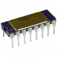
IC AMP INST 25MHZ PREC LN 16CDIP
Manufacturer
Analog Devices Inc
Datasheet
1.AD624ADZ.pdf
(16 pages)
Specifications of AD624BDZ
Amplifier Type
Instrumentation
Number Of Circuits
1
Slew Rate
5 V/µs
Gain Bandwidth Product
25MHz
-3db Bandwidth
1MHz
Current - Input Bias
25nA
Voltage - Input Offset
75µV
Current - Supply
3.5mA
Voltage - Supply, Single/dual (±)
±6 V ~ 18 V
Operating Temperature
-25°C ~ 85°C
Mounting Type
Through Hole
Package / Case
16-CDIP (0.300", 7.62mm)
No. Of Amplifiers
1
Input Offset Voltage
75µV
Gain Db Min
1dB
Bandwidth
25MHz
Amplifier Output
Single Ended
Cmrr
120dB
Supply Voltage Range
± 6V To ± 18V
Rohs Compliant
Yes
Lead Free Status / RoHS Status
Lead free / RoHS Compliant
Output Type
-
Current - Output / Channel
-
Available stocks
Company
Part Number
Manufacturer
Quantity
Price

Part Number:
AD624BDZ
Manufacturer:
ADI/亚德诺
Quantity:
20 000


AD624
AUTOZERO CIRCUITS
In many applications it is necessary to provide very accurate
data in high gain configurations. At room temperature the offset
effects can be nulled by the use of offset trimpots. Over the
operating temperature range, however, offset nulling becomes a
problem. The circuit of Figure 41 shows a CMOS DAC operat-
ing in the bipolar mode and connected to the reference terminal
to provide software controllable offset adjustments.
INPUTS
(–INPUT)
(+INPUT)
G = 200
G = 500
DATA
+INPUT
G = 100
–INPUT
–V
–INPUT
+INPUT
WR
RG
RG
S
CS
DAC A/DAC B
G = 500
AD589
1
2
G = 100
G = 200
39k
MSB
LSB
RG
INPUTS
RG
2
DATA
1
225.3
124
80.2
WR
CS
AD7524
50
50
+V
4445.7
S
GND
AD624
–V
+V
DB7
DB0
S
S
R
OUT1
OUT2
+V
AD7528
FB
DAC B
DAC A
S
V
B
C1
V
20k
20k
REF
AD712
10k
10k
1/2
+V
AD712
V
OUT
AD624
1/2
S
256:1
10k
20k
10k
10k
R4
AD712
R3
5k
1/2
R6
20k
R5
–V
AD712
1/2
S
V
OUT
In many applications complex software algorithms for autozero
applications are not available. For these applications Figure 42
provides a hardware solution.
The microprocessor controlled data acquisition system shown in
Figure 43 includes includes both autozero and autogain capabil-
ity. By dedicating two of the differential inputs, one to ground
and one to the A/D reference, the proper program calibration
cycles can eliminate both initial accuracy errors and accuracy
errors over temperature. The autozero cycle, in this application,
converts a number that appears to be ground and then writes
that same number (8 bit) to the AD624 which eliminates the
zero error since its output has an inverted scale. The autogain
cycle converts the A/D reference and compares it with full scale.
A multiplicative correction factor is then computed and applied
to subsequent readings.
15 16
14
13
AD7507
EN A1
LATCH
A0
ZERO PULSE
A2
RG
RG
2
1
RG
RG
AD712
GND
V
V
1/2
DD
200 s
1
SS
2
20k
AD624
AD624
ADDRESS BUS
+V
–V
10k
5k
S
S
A1
AD712
1/2
20k
0.1 F LOW
LEAKAGE
A2
AD542
AD583
AD7524
–V
A3
REF
1k
AGND
DECODE
V
12 11
A4
IN
CONTROL
AD574A
AD7510DIKD
9 10
V
REF
PROCESSOR
MICRO-
CH
V
OUT
Related parts for AD624BDZ
Image
Part Number
Description
Manufacturer
Datasheet
Request
R

Part Number:
Description:
±1.7g Dual-Axis IMEMS Accelerometer Evaluation Board
Manufacturer:
Analog Devices Inc
Datasheet:

Part Number:
Description:
Inertial Sensor Evaluation System
Manufacturer:
Analog Devices Inc
Datasheet:
Part Number:
Description:
Manufacturer:
Analog Devices Inc
Datasheet:
Part Number:
Description:
Manufacturer:
Analog Devices Inc
Datasheet:
Part Number:
Description:
Manufacturer:
Analog Devices Inc
Datasheet:
Part Number:
Description:
Manufacturer:
Analog Devices Inc
Datasheet:
Part Number:
Description:
Manufacturer:
Analog Devices Inc
Datasheet:
Part Number:
Description:
Manufacturer:
Analog Devices Inc
Datasheet:
Part Number:
Description:
Manufacturer:
Analog Devices Inc
Datasheet:
Part Number:
Description:
Manufacturer:
Analog Devices Inc
Datasheet:
Part Number:
Description:
Manufacturer:
Analog Devices Inc
Datasheet:
Part Number:
Description:
Manufacturer:
Analog Devices Inc
Datasheet:
Part Number:
Description:
Manufacturer:
Analog Devices Inc
Datasheet: