AD624BDZ Analog Devices Inc, AD624BDZ Datasheet - Page 7
AD624BDZ
Manufacturer Part Number
AD624BDZ
Description
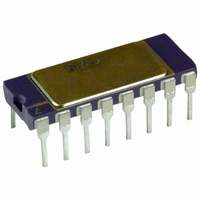
IC AMP INST 25MHZ PREC LN 16CDIP
Manufacturer
Analog Devices Inc
Datasheet
1.AD624ADZ.pdf
(16 pages)
Specifications of AD624BDZ
Amplifier Type
Instrumentation
Number Of Circuits
1
Slew Rate
5 V/µs
Gain Bandwidth Product
25MHz
-3db Bandwidth
1MHz
Current - Input Bias
25nA
Voltage - Input Offset
75µV
Current - Supply
3.5mA
Voltage - Supply, Single/dual (±)
±6 V ~ 18 V
Operating Temperature
-25°C ~ 85°C
Mounting Type
Through Hole
Package / Case
16-CDIP (0.300", 7.62mm)
No. Of Amplifiers
1
Input Offset Voltage
75µV
Gain Db Min
1dB
Bandwidth
25MHz
Amplifier Output
Single Ended
Cmrr
120dB
Supply Voltage Range
± 6V To ± 18V
Rohs Compliant
Yes
Lead Free Status / RoHS Status
Lead free / RoHS Compliant
Output Type
-
Current - Output / Channel
-
Available stocks
Company
Part Number
Manufacturer
Quantity
Price

Part Number:
AD624BDZ
Manufacturer:
ADI/亚德诺
Quantity:
20 000


THEORY OF OPERATION
The AD624 is a monolithic instrumentation amplifier based on
a modification of the classic three-op-amp instrumentation
amplifier. Monolithic construction and laser-wafer-trimming
allow the tight matching and tracking of circuit components and
the high level of performance that this circuit architecture is ca-
pable of.
A preamp section (Q1–Q4) develops the programmed gain by
the use of feedback concepts. Feedback from the outputs of A1
and A2 forces the collector currents of Q1–Q4 to be constant
thereby impressing the input voltage across R
The gain is set by choosing the value of R
Gain =
ance of the input preamp stage increasing it asymptotically to
the transconductance of the input transistors as R
for larger gains. This has three important advantages. First, this
approach allows the circuit to achieve a very high open loop gain
of 3 × 10
related errors to a negligible 3 ppm. Second, the gain bandwidth
product which is determined by C3 or C4 and the input trans-
conductance, reaches 25 MHz. Third, the input voltage noise
reduces to a value determined by the collector current of the
input transistors for an RTI noise of 4 nV/√Hz at G ≥ 500.
INPUT CONSIDERATIONS
Under input overload conditions the user will see R
and two diode drops (~1.2 V) between the plus and minus
inputs, in either direction. If safe overload current under all
conditions is assumed to be 10 mA, the maximum overload
voltage is ~ ± 2.5 V. While the AD624 can withstand this con-
tinuously, momentary overloads of ± 10 V will not harm the
device. On the other hand the inputs should never exceed the
supply voltage.
RG
100
200
500
2
40 k
8
R
at a programmed gain of 1000 thus reducing gain
G
AD624
–V
+V
+ 1. The value of R
S
S
G500
16.2k
1 F
20V p-p
INPUT
G1, 100, 200
100
AD712
G
1/2
+V
also sets the transconduct-
S
9.09k
100k
1k
0.1%
1%
1k
G
1 F
500
0.1%
from the equation,
G
1.62M
.
AD712
200
0.1%
G
1/2
–V
G
is reduced
S
1 F
1.82k
+ 100 Ω
16.2k
G = 100
G = 200
G = 500
RG
RG
The AD524 should be considered in applications that require
protection from severe input overload. If this is not possible,
external protection resistors can be put in series with the inputs
of the AD624 to augment the internal (50 Ω) protection resis-
tors. This will most seriously degrade the noise performance.
For this reason the value of these resistors should be chosen to
be as low as possible and still provide 10 mA of current limiting
under maximum continuous overload conditions. In selecting
the value of these resistors, the internal gain setting resistor and
the 1.2 volt drop need to be considered. For example, to pro-
tect the device from a continuous differential overload of 20 V
at a gain of 100, 1.9 kΩ of resistance is required. The internal
gain resistor is 404 Ω; the internal protect resistor is 100 Ω.
There is a 1.2 V drop across D1 or D2 and the base-emitter
junction of either Q1 and Q3 or Q2 and Q4 as shown in Figure
27, 1400 Ω of external resistance would be required (700 Ω in
series with each input). The RTI noise in this case would be
INPUT OFFSET AND OUTPUT OFFSET
Voltage offset specifications are often considered a figure of
merit for instrumentation amplifiers. While initial offset may
be adjusted to zero, shifts in offset voltage due to temperature
variations will cause errors. Intelligent systems can often correct
for this factor with an autozero cycle, but there are many small-
signal high-gain applications that don’t have this capability.
Voltage offset and offset drift each have two components; input
and output. Input offset is that component of offset that is
–IN
1
2
4 KTR
50
50 A
10k
13
1%
AD624
ext
+V
–V
Q1, Q3
+(4 nV / Hz )
4445
S
S
I1
50 A
C3
1k
10T
A1
225.3
80.2
124
R57
20k
RG
10k
+V
1%
VB
1
S
500
200
100
RG
2
2
= 6.2 nV / Hz
–V
A2
V
R56
20k
S
OUT
50 A
C4
I4
Q2,
Q4
I2
50 A
10k
10k
R53
R54
50
AD624
10k
10k
R52
A3
R55
SENSE
V
+IN
REF
O
Related parts for AD624BDZ
Image
Part Number
Description
Manufacturer
Datasheet
Request
R

Part Number:
Description:
±1.7g Dual-Axis IMEMS Accelerometer Evaluation Board
Manufacturer:
Analog Devices Inc
Datasheet:

Part Number:
Description:
Inertial Sensor Evaluation System
Manufacturer:
Analog Devices Inc
Datasheet:
Part Number:
Description:
Manufacturer:
Analog Devices Inc
Datasheet:
Part Number:
Description:
Manufacturer:
Analog Devices Inc
Datasheet:
Part Number:
Description:
Manufacturer:
Analog Devices Inc
Datasheet:
Part Number:
Description:
Manufacturer:
Analog Devices Inc
Datasheet:
Part Number:
Description:
Manufacturer:
Analog Devices Inc
Datasheet:
Part Number:
Description:
Manufacturer:
Analog Devices Inc
Datasheet:
Part Number:
Description:
Manufacturer:
Analog Devices Inc
Datasheet:
Part Number:
Description:
Manufacturer:
Analog Devices Inc
Datasheet:
Part Number:
Description:
Manufacturer:
Analog Devices Inc
Datasheet:
Part Number:
Description:
Manufacturer:
Analog Devices Inc
Datasheet:
Part Number:
Description:
Manufacturer:
Analog Devices Inc
Datasheet: