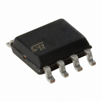
LM358DT STMicroelectronics, LM358DT Datasheet - Page 3

LM358DT
Manufacturer Part Number
LM358DT
Description
IC OP AMP LOW PWR DUAL 8-SOIC
Manufacturer
STMicroelectronics
Type
General Purpose Amplifierr
Specifications of LM358DT
Amplifier Type
General Purpose
Number Of Circuits
2
Slew Rate
0.6 V/µs
Gain Bandwidth Product
1.1MHz
Current - Input Bias
20nA
Voltage - Input Offset
2000µV
Current - Supply
700µA
Current - Output / Channel
60mA
Voltage - Supply, Single/dual (±)
3 V ~ 30 V, ±1.5 V ~ 15 V
Operating Temperature
0°C ~ 70°C
Mounting Type
Surface Mount
Package / Case
8-SOIC (3.9mm Width)
Number Of Channels
2
Common Mode Rejection Ratio (min)
70 dB
Input Offset Voltage
7 mV
Input Bias Current (max)
150 nA
Operating Supply Voltage
5 V, 9 V, 12 V, 15 V
Supply Current
1.2 mA
Maximum Power Dissipation
500 mW
Maximum Operating Temperature
+ 70 C
Minimum Operating Temperature
0 C
Dual Supply Voltage
+/- 3 V, +/- 5 V, +/- 9 V, +/- 12 V
Maximum Dual Supply Voltage
+/- 15 V
Minimum Dual Supply Voltage
+/- 1.5 V
Mounting Style
SMD/SMT
Shutdown
No
Supply Voltage (max)
30 V
Supply Voltage (min)
3 V
Technology
Bipolar
Voltage Gain Db
100 dB
Bandwidth
1.1 MHz
Channel Separation
120
Common Mode Rejection Ratio
85
Current, Input Bias
20 nA
Current, Input Offset
2 nA
Current, Output
40 mA
Current, Supply
0.7 mA
Harmonic Distortion
0.02 %
Number Of Amplifiers
Dual
Package Type
SO-8
Signal Gain
100 V/mV
Temperature, Operating, Range
0 to +70 °C
Voltage, Input
32 V
Voltage, Noise
55 nV/sqrt Hz
Voltage, Offset
2 mV
Voltage, Output, High
28 V
Voltage, Output, Low
5 mV
Voltage, Supply
3 to 30 V
Rail/rail I/o Type
No
Number Of Elements
2
Unity Gain Bandwidth Product
1.1MHz
Input Bias Current
150nA
Single Supply Voltage (typ)
5/9/12/15/18/24/28V
Dual Supply Voltage (typ)
±3/±5/±9/±12V
Voltage Gain In Db
100dB
Power Supply Requirement
Single/Dual
Shut Down Feature
No
Single Supply Voltage (min)
3V
Single Supply Voltage (max)
30V
Dual Supply Voltage (min)
±1.5V
Dual Supply Voltage (max)
±15V
Operating Temp Range
0C to 70C
Operating Temperature Classification
Commercial
Mounting
Surface Mount
Pin Count
8
Lead Free Status / RoHS Status
Lead free / RoHS Compliant
Output Type
-
-3db Bandwidth
-
Lead Free Status / Rohs Status
Lead free / RoHS Compliant
Other names
497-1591-2
Available stocks
Company
Part Number
Manufacturer
Quantity
Price
Company:
Part Number:
LM358DT
Manufacturer:
ST
Quantity:
16 700
Company:
Part Number:
LM358DT
Manufacturer:
ST
Quantity:
322 500
Part Number:
LM358DT
Manufacturer:
ST
Quantity:
20 000
LM158-LM258-LM358
2
Absolute maximum ratings
Table 1.
1. Short-circuits from the output to V
2. This input current only exists when the voltage at any of the input leads is driven negative. It is due to the
3. Short-circuits can cause excessive heating and destructive dissipation. R
4. Human body model: a 100 pF capacitor is charged to the specified voltage, then discharged through a
5. Machine model: a 200 pF capacitor is charged to the specified voltage, then discharged directly between
6. Charged device model: all pins and the package are charged together to the specified voltage and then
Symbol
T
R
ESD
R
V
T
current is approximately 40 mA independent of the magnitude of V
from simultaneous short circuits on all amplifiers.
collector-base junction of the input PNP transistor becoming forward-biased and thereby acting as input
diode clamp. In addition to this diode action, there is NPN parasitic action on the IC chip. This transistor
action can cause the output voltages of the Op-amps to go to the V
overdrive) for the time during which an input is driven negative.
This is not destructive and normal output is restored for input voltages above -0.3 V.
1.5 kΩ resistor between two pins of the device. This is done for all couples of connected pin combinations
while the other pins are floating.
two pins of the device with no external series resistor (internal resistor < 5 Ω). This is done for all couples of
connected pin combinations while the other pins are floating.
discharged directly to the ground through only one pin. This is done for all pins.
V
oper
V
I
T
CC
thja
thjc
stg
in
id
j
i
Supply voltage
Input voltage
Differential input voltage
Output short-circuit duration
Input current
Operating free-air temperature range
Storage temperature range
Maximum junction temperature
Thermal resistance junction to ambient
Thermal resistance junction to case
HBM: human body model
MM: machine model
CDM: charged device model
SO-8
MiniSO-8
TSSOP8
DIP8
SO-8
MiniSO-8
TSSOP8
DIP8
Absolute maximum ratings
(2)
Parameter
(5)
CC
can cause excessive heating if V
(4)
(6)
(1)
(3)
(3)
-55 to +125 -40 to +105
LM158,A
5 mA in DC or 50 mA in AC (duty
CC
CC
. Destructive dissipation can result
cycle = 10%, T=1s)
voltage level (or to ground for a large
CC
> 15 V. The maximum output
th
-65 to +150
Absolute maximum ratings
+/-16 or 32
are typical values.
LM258,A
Infinite
150
125
190
120
300
200
1.5
32
32
85
40
39
37
41
LM358,A
0 to +70
°C/W
°C/W
Unit
mA
kV
°C
°C
°C
V
V
V
V
V
3/19


