HFA1412IBZ Intersil, HFA1412IBZ Datasheet
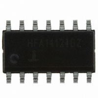
IC BUFFER QUAD 350MHZ LP 14-SOIC

HFA1412IBZ

Manufacturer Part Number
HFA1412IBZ
Description
IC BUFFER QUAD 350MHZ LP 14-SOIC
Manufacturer
Intersil
Datasheet

Specifications of HFA1412IBZ

Amplifier Type
Buffer
Number Of Circuits
4
Slew Rate
1700 V/µs
-3db Bandwidth
350MHz
Current - Input Bias
1µA
Voltage - Input Offset
2000µV
Current - Supply
5.9mA
Current - Output / Channel
55mA
Voltage - Supply, Single/dual (±)
9 V ~ 11 V, ±4.5 V ~ 5.5 V
Operating Temperature
-40°C ~ 85°C
Mounting Type
Surface Mount
Package / Case
14-SOIC (3.9mm Width), 14-SOL
Rohs Compliant
YES
Lead Free Status / RoHS Status
Lead free / RoHS Compliant
Output Type
-
Gain Bandwidth Product
-

Available stocks

Company
Part Number
Manufacturer
Quantity
Price
Part Number:
HFA1412IBZ
Manufacturer:
INTERSIL
Quantity:
20 000
Quad, 350MHz, Low Power,
Programmable Gain Buffer Amplifier
The HFA1412 is a quad closed loop Buffer featuring user
programmable gain and high speed video performance.
A unique feature of the HFA1412’s pinout allows the user to
select a voltage gain of +1, -1, or +2 (see the “Application
Information” section). The on-chip gain setting resistors
eliminate eight external resistors, thus saving board space or
freeing up space for termination resistors. The on-chip
feedback resistor is preset at the optimum value, and also
eliminates worries about parasitic feedback capacitance.
Additionally, the capacitance sensitive summing node is
buried inside the package where it is unaffected by PCB
parasitics. Compatibility with existing op amp pinouts
provides flexibility to upgrade low gain amplifiers, while
decreasing component count. Unlike most buffers, the
standard pinout provides an upgrade path should a higher
closed loop gain be needed at a future date.
The HFA1412 is an excellent choice for component and
composite video systems as indicated by the excellent gain
flatness, and 0.03%/0.02 Degree Differential Gain/Phase
specifications (R
with no external resistors makes it particularly desirable for
applications driving double terminated cables.
For Military product, refer to the HFA1412/883 data sheet.
Ordering Information
HFA1412IP
HFA1412IPZ
(Note)
HFA1412IB
HFA1412IBZ
(Note)
HA5025EVAL
*Pb-free PDIPs can be used for through hole wave solder
processing only. They are not intended for use in Reflow solder
processing applications.
NOTE: Intersil Pb-free plus anneal products employ special Pb-free
material sets; molding compounds/die attach materials and 100%
matte tin plate termination finish, which are RoHS compliant and
compatible with both SnPb and Pb-free soldering operations. Intersil
Pb-free products are MSL classified at Pb-free peak reflow
temperatures that meet or exceed the Pb-free requirements of
IPC/JEDEC J STD-020.
NUMBER
PART
HFA1412IP
HFA1412IPZ
HFA1412IB
HFA1412IBZ
L
MARKING
= 150Ω). Its ability to deliver a gain of +2
PART
®
DIP Evaluation Board For Quad Op
Amp
-40 to 85 14 Ld PDIP
-40 to 85 14 Ld PDIP*
-40 to 85 14 Ld SOIC
1
RANGE
TEMP.
(°C)
Data Sheet
(Pb-free)
(Pb-free)
PACKAGE
DWG. #
E14.3
E14.3
M14.15
M14.15
1-888-INTERSIL or 1-888-468-3774
PKG.
CAUTION: These devices are sensitive to electrostatic discharge; follow proper IC Handling Procedures.
Features
• User Programmable For Closed-Loop Gains of +1, -1 or
• Wide -3dB Bandwidth. . . . . . . . . . . . . . . . . . . . . . 350MHz
• Low Supply Current . . . . . . . . . . . . . . . . . . . . 6mA/Buffer
• Excellent Gain Flatness (to 100MHz). . . . . . . . . .
• Low Differential Gain and Phase . . . . 0.03%/0.02 Degree
• Very Fast Slew Rate . . . . . . . . . . . . . . . . . . . . . 1650V/µs
• Fast Settling Time (0.1%). . . . . . . . . . . . . . . . . . . . . 28ns
• High Output Current . . . . . . . . . . . . . . . . . . . . . . . . . 55mA
• Excellent Gain Accuracy . . . . . . . . . . . . . . . . . . . 0.99V/V
• Overdrive Recovery . . . . . . . . . . . . . . . . . . . . . . . . <10ns
• Standard Operational Amplifier Pinout
• Pb-Free Plus Anneal Available (RoHS Compliant)
Applications
• Video Distribution Amps
• Flash A/D Drivers
• Video Cable Drivers
• Video Switchers and Routers
• Medical Imaging Systems
• RGB Video Processing
• High Speed Oscilloscopes and Analyzers
Pinout
Functional Diagram
+2 Without Use of External Resistors
January 23, 2006
All other trademarks mentioned are the property of their respective owners.
+IN1
+IN2
+IN3
+IN4
|
-IN1
-IN2
-IN3
-IN4
Copyright Intersil Americas Inc. 1998, 2005, 2006. All Rights Reserved
Intersil (and design) is a registered trademark of Intersil Americas Inc.
10
13
12
OUT1
OUT2
2
3
6
5
9
+IN1
+IN2
-IN1
-IN2
V+
425
425
425
425
HFA1412 (PDIP, SOIC)
1
2
3
4
5
6
7
TOP VIEW
-
+
-
+
-
+
-
+
425
425
425
425
14
13
12
10
11
9
8
OUT4
-IN4
+IN4
V-
+IN3
-IN3
OUT3
1
7
8
14
HFA1412
OUT1
OUT2
OUT3
OUT4
FN4152.4
±
0.08dB

Related parts for HFA1412IBZ

HFA1412IBZ Summary of contents

Page 1

... Ld PDIP HFA1412IPZ HFA1412IPZ - PDIP* (Note) HFA1412IB HFA1412IB - SOIC HFA1412IBZ HFA1412IBZ - SOIC (Note) HA5025EVAL DIP Evaluation Board For Quad Op Amp *Pb-free PDIPs can be used for through hole wave solder processing only. They are not intended for use in Reflow solder processing applications. NOTE: Intersil Pb-free plus anneal products employ special Pb-free material sets ...

Page 2

Absolute Maximum Ratings Voltage Between V+ and 11V DC Input ...

Page 3

Electrical Specifications V SUPPLY PARAMETER Non-Inverting Input Noise Current Density (Note 4) TRANSFER CHARACTERISTICS Gain (V = -1V to +1V) IN Channel-to-Channel Gain Mismatch AC CHARACTERISTICS -3dB Bandwidth (V = 0.2V , Note 4) OUT P-P Full Power Bandwidth (V ...

Page 4

Electrical Specifications V SUPPLY PARAMETER Output Current (Note 4) Output Short Circuit Current DC Closed Loop Output Impedance Second Harmonic Distortion ( Note 4) V OUT P-P Third Harmonic Distortion (A = +2, V ...

Page 5

Application Information HFA1412 Advantages The HFA1412 features a novel design which allows the user to select from three closed loop gains, without any external components. The result is a more flexible product, fewer part types in inventory, and more efficient ...

Page 6

PC Board Layout This amplifier’s frequency response depends greatly on the care taken in designing the PC board (PCB). The use of low inductance components such as chip resistors and chip capacitors is strongly recommended, while a solid ground plane ...

Page 7

Typical Performance Curves 200 150 100 50 0 -50 -100 -150 -200 TIME (5ns/DIV.) FIGURE 4. SMALL SIGNAL PULSE RESPONSE 200 150 100 50 0 -50 -100 -150 -200 TIME (5ns/DIV.) FIGURE ...

Page 8

Typical Performance Curves V = 200mV OUT P GAIN -3 -6 PHASE A 0 FREQUENCY (MHz) FIGURE 10. FREQUENCY RESPONSE 200mV V OUT P GAIN - ...

Page 9

Typical Performance Curves GAIN - PHASE 4V P-P 2.5V 0 FREQUENCY (MHz) FIGURE 16. FREQUENCY RESPONSE FOR VARIOUS OUTPUT VOLTAGES 450 400 350 A ...

Page 10

Typical Performance Curves - -45 -50 10MHz -55 -60 -65 -70 -75 - OUTPUT POWER (dBm) FIGURE 22. 2nd HARMONIC DISTORTION -45 -50 -55 10MHz ...

Page 11

Typical Performance Curves +0.5V OUT 100 500 900 1300 INPUT TRANSITION TIME (ps) FIGURE 28. OVERSHOOT vs TRANSITION TIME 0.5V OUT P-P ...

Page 12

Typical Performance Curves 6.6 6.5 6.4 6.3 6.2 6.1 6.0 5.9 5.8 5.7 5.6 5.5 4.5 5 5.5 SUPPLY VOLTAGE (±V) FIGURE 34. SUPPLY CURRENT vs SUPPLY VOLTAGE 12 HFA1412 = ±5V 25° 100Ω, Unless ...

Page 13

... Accordingly, the reader is cautioned to verify that data sheets are current before placing orders. Information furnished by Intersil is believed to be accurate and reliable. However, no responsibility is assumed by Intersil or its subsidiaries for its use; nor for any infringements of patents or other rights of third parties which may result from its use ...

Related keywords