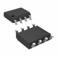
LMP8602MA/NOPB National Semiconductor, LMP8602MA/NOPB Datasheet - Page 14

LMP8602MA/NOPB
Manufacturer Part Number
LMP8602MA/NOPB
Description
IC AMP CURRENT SENSE 60V 8SOIC
Manufacturer
National Semiconductor
Series
LMP®r
Type
Current Sense Amplifierr
Datasheet
1.LMP8602MMENOPB.pdf
(24 pages)
Specifications of LMP8602MA/NOPB
Amplifier Type
Current Sense
Number Of Circuits
1
Slew Rate
0.83 V/µs
Gain Bandwidth Product
60kHz
Current - Input Bias
0.04pA
Voltage - Input Offset
150µV
Current - Supply
1.1mA
Current - Output / Channel
48mA
Voltage - Supply, Single/dual (±)
3 V ~ 5.5 V
Operating Temperature
-40°C ~ 125°C
Mounting Type
Surface Mount
Package / Case
8-SOIC (3.9mm Width)
No. Of Amplifiers
1
Input Bias Current
20nA
Input Offset Voltage
1mV
Bandwidth
60kHz
Cmrr
105dB
Supply Voltage Range
3V To 5.5V
Supply Current
1.3mA
Rohs Compliant
Yes
Number Of Channels
1
Number Of Elements
2
Power Supply Requirement
Single
Common Mode Rejection Ratio
80dB
Voltage Gain Db
34.02dB
Single Supply Voltage (typ)
5V
Dual Supply Voltage (typ)
Not RequiredV
Power Supply Rejection Ratio
70dB
Rail/rail I/o Type
No
Single Supply Voltage (min)
3V
Single Supply Voltage (max)
5.5V
Dual Supply Voltage (min)
Not RequiredV
Dual Supply Voltage (max)
Not RequiredV
Operating Temp Range
-40C to 125C
Operating Temperature Classification
Automotive
Mounting
Surface Mount
Pin Count
8
Package Type
SOIC N
Lead Free Status / RoHS Status
Lead free / RoHS Compliant
Output Type
-
-3db Bandwidth
-
Lead Free Status / Rohs Status
Compliant
Other names
LMP8602MA
Available stocks
Company
Part Number
Manufacturer
Quantity
Price
Company:
Part Number:
LMP8602MA/NOPB
Manufacturer:
National Semiconductor
Quantity:
135
www.national.com
Application Information
GENERAL
The LMP8602 and LMP8603 are fixed gain differential volt-
age precision amplifiers with a gain of 50x for the LMP8602,
and 100x for the LMP8603. The input common mode voltage
range is -22V to +60V when operating from a single 5V supply
or -4V to +27V input common mode voltage range when op-
erating from a single 3.3V supply. The LMP8602 and
LMP8603 are members of the LMP family and are ideal parts
for unidirectional and bidirectional current sensing applica-
tions. Because of the proprietary chopping level-shift input
stage the LMP8602 and LMP8603 achieve very low offset,
very low thermal offset drift, and very high CMRR. The
LMP8602 and LMP8603 will amplify and filter small differen-
tial signals in the presence of high common mode voltages.
The LMP8602/LMP8602Q/LMP8603/LMP8603Q use level
shift resistors at the inputs. Because of these resistors, the
LMP8602/LMP8602Q/LMP8603/LMP8603Q can easily with-
stand very large differential input voltages that may exist in
fault conditions where some other less protected high-perfor-
mance current sense amplifiers might sustain permanent
damage.
PERFORMANCE GUARANTIES
To guaranty the high performance of the LMP8602/LM-
P8602Q/LMP8603/LMP8603Q, all minimum and maximum
values shown in the parameter tables of this datasheet are
100% tested where all bold limits are also 100% tested over
temperature.
FIGURE 1. Theory of Operation
K2 = 5 for LMP8602, K2 = 10 for LMP8603
14
THEORY OF OPERATION
The schematic shown in
sentation of the internal operation of the LMP8602/
LMP8603.
The signal on the input pins is typically a small differential
voltage across a current sensing shunt resistor. The input
signal may appear at a high common mode voltage. The input
signals are accessed through two input resistors. The propri-
etary chopping level-shift current circuit pulls or pushes cur-
rent through the input resistors to bring the common mode
voltage behind these resistors within the supply rails. Subse-
quently, the signal is gained up by a factor of 10 (K1) and
brought out on the A1 pin through a trimmed 100 kΩ resistor.
In the application, additional gain adjustment or filtering com-
ponents can be added between the A1 and A2 pins as will be
explained in subsequent sections. The signal on the A2 pin is
further amplified by a factor (K2) which equals a factor of 5 for
the LMP8602 and a factor of 10 for the LMP8603. The output
signal of the final gain stage is provided on the OUT pin. The
OFFSET pin allows the output signal to be level-shifted to
enable bidirectional current sensing as will be explained be-
low.
Figure 1
30083405
gives a schematic repre-


