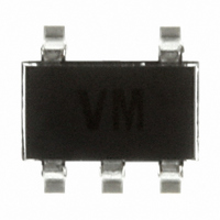
TSC101BILT STMicroelectronics, TSC101BILT Datasheet

TSC101BILT
Specifications of TSC101BILT
TSC101BILT
Available stocks
Related parts for TSC101BILT
TSC101BILT Summary of contents
Page 1
Features ■ Independent supply and input common-mode voltages ■ Wide common-mode operating range: 2 ■ Wide common-mode surviving range: -0 (load-dump) ■ Wide supply voltage range ■ Low current consumption: ...
Page 2
Application schematics and pin description 1 Application schematics and pin description The TSC101 high-side current sense amplifier features a 2 input common-mode range that is independent of the supply voltage. The main advantage of this feature is ...
Page 3
TSC101 2 Absolute maximum ratings and operating conditions Table 2. Absolute maximum ratings Symbol V Input pins differential voltage ( Input pin voltages ( supply voltage output pin voltage out T Storage ...
Page 4
Electrical characteristics 3 Electrical characteristics (1) Table 4. Supply Symbol Parameter I Total supply current CC 1. Unless otherwise specified, the test conditions are T on Out. (1) Table 5. Input Symbol Parameter Common mode rejection CMR Variation of V ...
Page 5
TSC101 (1) Table 6. Output Symbol Parameter Av Gain ΔAv Gain accuracy ΔV /ΔT Output voltage drift vs. T out ΔV /ΔI Output stage load regulation out out ΔV Total output voltage accuracy out ΔV Total output voltage accuracy out ...
Page 6
Electrical characteristics Table 7. Frequency response Symbol Parameter ts Output settling to 1% final value SR Slew rate BW 3dB bandwidth 1. Unless otherwise specified, the test conditions are T on Out. 2. For stability purposes not recommend ...
Page 7
TSC101 3.1 Electrical characteristics curves For the following curves, the tested device is a TSC101C, and the test conditions are T = 25°C, V amb CC otherwise specified. Figure 2. Supply current vs. supply voltage ( sense ...
Page 8
Electrical characteristics Figure 6. Minimum common mode operating voltage vs. temperature Figure 8. Output stage high-state saturation voltage versus output current ( sense 8/18 Figure 7. Output stage low-state saturation voltage versus output current (V sense Figure ...
Page 9
TSC101 Figure 10. Output short-circuit sink current versus temperature (Out pin connected Figure 12. Input offset drift versus temperature Figure 14. Bode diagram (V Figure 11. Output stage load regulation ) Figure 13. Output voltage drift versus ...
Page 10
Electrical characteristics Figure 16. Total output voltage accuracy versus V sense Figure 18. Output voltage versus V for low V values) sense 10/18 Figure 17. Output voltage versus V (detail Figure 19. Step response sense Doc ID 13313 Rev 3 ...
Page 11
TSC101 4 Parameter definitions 4.1 Common mode rejection ratio (CMR) The common-mode rejection ratio (CMR) measures the ability of the current-sensing amplifier to reject any DC voltage applied on both inputs V back to the input so that its effect ...
Page 12
Parameter definitions Figure 20. V out 4.4 Output voltage drift versus temperature The output voltage drift versus temperature is defined as the maximum variation of V respect to its value at 25°C, over the temperature range calculated as ...
Page 13
TSC101 4.5 Output voltage accuracy The output voltage accuracy is the difference between the actual output voltage and the theoretical output voltage. Ideally, the current sensing output voltage should be equal to the input differential voltage multiplied by the theoretical ...
Page 14
Application information 5 Application information The TSC101 can be used to measure current and to feed back the information to a microcontroller, as shown in Figure 23. Typical application schematic The current from the supply flows to the load through ...
Page 15
TSC101 6 Package information In order to meet environmental requirements, ST offers these devices in different grades of ® ECOPACK packages, depending on their level of environmental compliance. ECOPACK specifications, grade definitions and product status are available at: www.st.com. ® ...
Page 16
... Ordering information 7 Ordering information Table 10. Order codes Temperature Part number range TSC101AILT TSC101BILT -40°C, +125°C TSC101CILT (1) TSC101AIYLT (1) TSC101BIYLT -40°C, +125°C (1) TSC101CIYLT 1. Qualified and characterized according to AEC Q100 and Q003 or equivalent, advanced screening according to AEC Q001 & Q 002 or equivalent. 16/18 ...
Page 17
TSC101 8 Revision history Table 11. Document revision history Date 05-Mar-2007 22-Oct-2007 14-Mar-2011 Revision 1 First release, preliminary data. Document status promoted from preliminary data to datasheet. 2 Added test results in electrical characteristics tables. Added electrical characteristics curves. Added ...
Page 18
... Information in this document is provided solely in connection with ST products. STMicroelectronics NV and its subsidiaries (“ST”) reserve the right to make changes, corrections, modifications or improvements, to this document, and the products and services described herein at any time, without notice. All ST products are sold pursuant to ST’s terms and conditions of sale. ...


