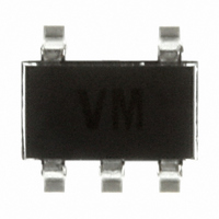
TSC101BILT STMicroelectronics, TSC101BILT Datasheet - Page 3

TSC101BILT
Manufacturer Part Number
TSC101BILT
Description
IC AMP HISIDE CURR SENSE SOT23-5
Manufacturer
STMicroelectronics
Specifications of TSC101BILT
Mfg Application Notes
TSC101 AppNote
Amplifier Type
Current Sense
Number Of Circuits
1
Slew Rate
0.9 V/µs
-3db Bandwidth
670kHz
Current - Input Bias
5.5µA
Voltage - Input Offset
200µV
Current - Supply
165µA
Current - Output / Channel
60mA
Voltage - Supply, Single/dual (±)
4 V ~ 24 V
Operating Temperature
-40°C ~ 125°C
Mounting Type
Surface Mount
Package / Case
SOT-23-5, SC-74A, SOT-25
Number Of Channels
Single
Common Mode Rejection Ratio (min)
90 dB
Available Set Gain
33.98 dB (Typ)
Input Offset Voltage
1.5 mV
Input Bias Current (max)
8 uA
Operating Supply Voltage
5 V, 9 V, 12 V, 15 V, 18 V
Supply Current
0.3 mA
Maximum Operating Temperature
+ 125 C
Minimum Operating Temperature
- 40 C
Mounting Style
SMD/SMT
Supply Voltage (max)
24 V
Supply Voltage (min)
4 V
No. Of Amplifiers
1
Input Bias Current
8µA
Output Current Per Channel
60mA
Gain Db Max
50dB
Bandwidth
500kHz
Cmrr
105dB
Supply Voltage Range
4V
Rohs Compliant
Yes
For Use With
497-8339 - BOARD EVAL BASED ON TSC101
Lead Free Status / RoHS Status
Lead free / RoHS Compliant
Output Type
-
Gain Bandwidth Product
-
Lead Free Status / Rohs Status
Lead free / RoHS Compliant
Other names
497-6946-2
TSC101BILT
TSC101BILT
Available stocks
Company
Part Number
Manufacturer
Quantity
Price
Company:
Part Number:
TSC101BILT
Manufacturer:
STM
Quantity:
29 203
Part Number:
TSC101BILT
Manufacturer:
ST
Quantity:
20 000
TSC101
2
Absolute maximum ratings and operating conditions
Table 2.
1. Voltage values are measured with respect to the ground pin.
2. Human body model: a 100 pF capacitor is charged to the specified voltage, then discharged through a
3. Machine model: a 200 pF capacitor is charged to the specified voltage, then discharged directly between
4. Charged device model: all pins plus package are charged together to the specified voltage and then
Table 3.
Symbol
Symbol
1.5kΩ resistor between two pins of the device. This is done for all couples of connected pin combinations
while the other pins are floating.
two pins of the device with no external series resistor (internal resistor < 5 Ω). This is done for all couples of
connected pin combinations while the other pins are floating.
discharged directly to the ground.
ESD
T
R
V
V
V
V
T
V
oper
V
T
thja
icm
CC
out
stg
CC
id
i
j
Absolute maximum ratings
Operating conditions
Input pins differential voltage (V
Input pin voltages (V
DC supply voltage
DC output pin voltage
Storage temperature
Maximum junction temperature
SOT23-5 thermal resistance junction to ambient
HBM: human body model
MM: machine model
CDM: charged device model
DC supply voltage from T
Operational temperature range (T
Common mode voltage range
(1)
Doc ID 13313 Rev 3
Parameter
Parameter
(3)
p
(1)
and V
Absolute maximum ratings and operating conditions
(2)
min
m
(4)
to T
)
(1)
p
-V
max
min
m
)
to T
max
)
-0.3 to V
-55 to 150
-40 to 125
-0.3 to 60
-0.3 to 25
4.0 to 24
2.8 to 30
Value
Value
±60
150
250
150
2.5
1.5
CC
°C/W
Unit
Unit
°C
°C
kV
kV
°C
V
V
V
V
V
V
V
3/18


