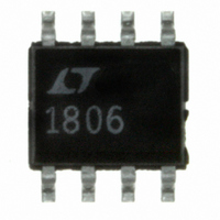
LT1806CS8 Linear Technology, LT1806CS8 Datasheet - Page 11

LT1806CS8
Manufacturer Part Number
LT1806CS8
Description
IC OPAMP R-R IN/OUT SNGL 8-SOIC
Manufacturer
Linear Technology
Datasheet
1.LT1806CS8PBF.pdf
(28 pages)
Specifications of LT1806CS8
Amplifier Type
General Purpose
Number Of Circuits
1
Output Type
Rail-to-Rail
Slew Rate
140 V/µs
Gain Bandwidth Product
325MHz
Current - Input Bias
5µA
Voltage - Input Offset
100µV
Current - Supply
11mA
Current - Output / Channel
85mA
Voltage - Supply, Single/dual (±)
2.5 V ~ 12.6 V, ±1.25 V ~ 6.3 V
Operating Temperature
0°C ~ 70°C
Mounting Type
Surface Mount
Package / Case
8-SOIC (3.9mm Width)
Lead Free Status / RoHS Status
Contains lead / RoHS non-compliant
-3db Bandwidth
-
Available stocks
Company
Part Number
Manufacturer
Quantity
Price
Part Number:
LT1806CS8
Manufacturer:
LINEAR/凌特
Quantity:
20 000
Company:
Part Number:
LT1806CS8#PBF
Manufacturer:
LT
Quantity:
1 469
Part Number:
LT1806CS8#PBF
Manufacturer:
LT
Quantity:
20 000
Part Number:
LT1806CS8#TRPBF
Manufacturer:
LINEAR/凌特
Quantity:
20 000
ELECTRICAL CHARACTERISTICS
temperature range. V
SYMBOL
t
GBW
SR
FPBW
Note 1: Stresses beyond those listed under Absolute Maximum Ratings
may cause permanent damage to the device. Exposure to any Absolute
Maximum Rating condition for extended periods may affect device
reliability and lifetime.
Note 2: The inputs are protected by back-to-back diodes. If the differential
input voltage exceeds 1.4V, the input current should be limited to less
than 10mA. This parameter is guaranteed to meet specifi ed performance
through design and/or characterization. It is not 100% tested.
Note 3: A heat sink may be required to keep the junction temperature below
the absolute maximum rating when the output is shorted indefi nitely.
Note 4: The LT1806C/LT1806I and LT1807C/LT1807I are guaranteed
functional over the temperature range of –40°C and 85°C.
Note 5: The LT1806C/LT1807C are guaranteed to meet specifi ed
performance from 0°C to 70°C. The LT1806C/LT1807C are designed,
TYPICAL PERFORMANCE CHARACTERISTICS
OFF
50
40
10
30
20
0
–500
V
(PNP Stage)
V
V
OS
S
CM
PARAMETER
Turn-Off Time
Gain-Bandwidth Product
Slew Rate
Full-Power Bandwidth
= 5V, 0V
Distribution, V
= 0V
–300
INPUT OFFSET VOLTAGE (μV)
–100
S
= ±5V, V
CM
100
= 0V
SHDN
300
= open; V
18067 G01
500
CM
= 0V, V
10
50
40
30
20
0
–500
V
(NPN Stage)
V
V
CONDITIONS
V
Frequency = 6MHz
A
Measure at V
V
OS
S
CM
SHDN
V
O
= 5V, 0V
OUT
= –1, R
= 8V
Distribution, V
= 5V
The
–300
INPUT OFFSET VOLTAGE (μV)
= 4.5V to 0.3V, R
P-P
= 0V, unless otherwise noted. (Note 5)
l
L
denotes the specifi cations which apply over the −40°C < T
= 1k, V
–100
O
= ±3V
characterized and expected to meet specifi ed performance from –40°C to
85°C but are not tested or QA sampled at these temperatures. The LT1806I/
LT1807I are guaranteed to meet specifi ed performance from –40°C to 85°C.
Note 6: Minimum supply voltage is guaranteed by power supply rejection
ratio test.
Note 7: Output voltage swings are measured between the output and
power supply rails.
Note 8: This parameter is not 100% tested.
Note 9: Thermal resistance varies depending upon the amount of PC board
metal attached to the V
amount of 2oz copper metal trace connecting to the V
the thermal resistance tables in the Applications Information section.
Note 10: Matching parameters are the difference between the two
amplifi ers of the LT1807.
O
CM
100
= ±4V,
= 5V
L
= 100Ω
300
18067 G02
500
–
pin of the device. θ
l
l
l
l
50
40
20
10
30
0
–500
ΔV
V
S
LT1806/LT1807
MIN
125
OS
= 5V, 0V
50
–300
Shift for V
INPUT OFFSET VOLTAGE (μV)
JA
is specifi ed for a certain
TYP
–100
290
100
50
4
CM
–
= 0V to 5V
100
pin as described in
MAX
A
300
< 85°C
11
18067 G03
UNITS
18067fc
MHz
MHz
V/μs
500
ns


