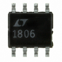
LT1806CS8 Linear Technology, LT1806CS8 Datasheet - Page 19

LT1806CS8
Manufacturer Part Number
LT1806CS8
Description
IC OPAMP R-R IN/OUT SNGL 8-SOIC
Manufacturer
Linear Technology
Datasheet
1.LT1806CS8PBF.pdf
(28 pages)
Specifications of LT1806CS8
Amplifier Type
General Purpose
Number Of Circuits
1
Output Type
Rail-to-Rail
Slew Rate
140 V/µs
Gain Bandwidth Product
325MHz
Current - Input Bias
5µA
Voltage - Input Offset
100µV
Current - Supply
11mA
Current - Output / Channel
85mA
Voltage - Supply, Single/dual (±)
2.5 V ~ 12.6 V, ±1.25 V ~ 6.3 V
Operating Temperature
0°C ~ 70°C
Mounting Type
Surface Mount
Package / Case
8-SOIC (3.9mm Width)
Lead Free Status / RoHS Status
Contains lead / RoHS non-compliant
-3db Bandwidth
-
Available stocks
Company
Part Number
Manufacturer
Quantity
Price
Part Number:
LT1806CS8
Manufacturer:
LINEAR/凌特
Quantity:
20 000
Company:
Part Number:
LT1806CS8#PBF
Manufacturer:
LT
Quantity:
1 469
Part Number:
LT1806CS8#PBF
Manufacturer:
LT
Quantity:
20 000
Part Number:
LT1806CS8#TRPBF
Manufacturer:
LINEAR/凌特
Quantity:
20 000
APPLICATIONS INFORMATION
The maximum ambient temperature that the part is
allowed to operate is:
To operate the device at higher ambient temperature,
connect more metal area to the V
resistance of the package as indicated in Table 2.
Input Offset Voltage
The offset voltage will change depending upon which
input stage is active and the maximum offset voltage is
guaranteed to less than 550μV. To maintain the precision
characteristics of the amplifi er, the change of V
entire input common mode range (CMRR) is limited to be
less than 550μV on a single 5V and 3V supply.
Input Bias Current
The input bias current polarity depends on a given input
common voltage at which the input stage is operating.
When the PNP input stage is active, the input bias currents
fl ow out of the input pins. When the NPN input stage is
activated, the input bias current fl ows into the input pins.
Because the input offset current is less than the input bias
current, matching the source resistances at the input pins
will reduce total offset error.
T
A
= T
= 150°C – (0.53W • 105°C/W) = 94°C
J
– (P
D(MAX)
• 105°C/W)
–
pin to reduce the thermal
OS
over the
Output
The LT1806/LT1807 can deliver a large output current, so
the short-circuit current limit is set around 85mA to prevent
damage to the device. Attention must be paid to keep the
junction temperature of the IC below the absolute maximum
rating of 150°C (refer to the Power Dissipation section)
when the output is continuously short circuited. The output
of the amplifi er has reverse-biased diodes connected to
each supply. If the output is forced beyond either supply,
unlimited current will fl ow through these diodes. If the
current is transient and limited to one hundred milliamps
or less, no damage to the device will occur.
Overdrive Protection
When the input voltage exceeds the power supplies, two
pairs of crossing diodes D1 to D4 will prevent the output
from reversing polarity. If the input voltage exceeds either
power supply by 700mV, diode D1/D2 or D3/D4 will turn
on to keep the output at the proper polarity. For the phase
reversal protection to perform properly, the input current
must be limited to less than 5mA. If the amplifi er is severely
overdriven, an external resistor should be used to limit
the overdrive current.
LT1806/LT1807
19
18067fc


