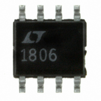
LT1806CS8 Linear Technology, LT1806CS8 Datasheet - Page 18

LT1806CS8
Manufacturer Part Number
LT1806CS8
Description
IC OPAMP R-R IN/OUT SNGL 8-SOIC
Manufacturer
Linear Technology
Datasheet
1.LT1806CS8PBF.pdf
(28 pages)
Specifications of LT1806CS8
Amplifier Type
General Purpose
Number Of Circuits
1
Output Type
Rail-to-Rail
Slew Rate
140 V/µs
Gain Bandwidth Product
325MHz
Current - Input Bias
5µA
Voltage - Input Offset
100µV
Current - Supply
11mA
Current - Output / Channel
85mA
Voltage - Supply, Single/dual (±)
2.5 V ~ 12.6 V, ±1.25 V ~ 6.3 V
Operating Temperature
0°C ~ 70°C
Mounting Type
Surface Mount
Package / Case
8-SOIC (3.9mm Width)
Lead Free Status / RoHS Status
Contains lead / RoHS non-compliant
-3db Bandwidth
-
Available stocks
Company
Part Number
Manufacturer
Quantity
Price
Part Number:
LT1806CS8
Manufacturer:
LINEAR/凌特
Quantity:
20 000
Company:
Part Number:
LT1806CS8#PBF
Manufacturer:
LT
Quantity:
1 469
Part Number:
LT1806CS8#PBF
Manufacturer:
LT
Quantity:
20 000
Part Number:
LT1806CS8#TRPBF
Manufacturer:
LINEAR/凌特
Quantity:
20 000
APPLICATIONS INFORMATION
LT1806/LT1807
or 8-lead MSOP package. All packages have the V
ply pin fused to the lead frame to enhance the thermal
conductance when connecting to a ground plane or a
large metal trace. Metal trace and plated through-holes
can be used to spread the heat generated by the device
to the backside of the PC board. For example, on a 3/32"
FR-4 board with 2oz copper, a total of 660 square mil-
limeters connects to Pin 4 of LT1807 in an SO-8 package
(330 square millimeters on each side of the PC board) will
bring the thermal resistance, θ
extra metal trace beside the power line connecting to the
V
around 105°C/W. More information on thermal resistance
for all packages with various metal areas connecting to
the V
Table 1. LT1806 6-Lead SOT-23 Package
Device is mounted on topside.
Table 2. LT1806/LT1807 SO-8 Package
Device is mounted on topside.
18
–
TOPSIDE
TOPSIDE (mm
COPPER AREA
(mm
pin to provide a heat sink, the thermal resistance will be
1100
330
35
35
0
COPPER AREA
–
2
270
100
pin is provided in Tables 1, 2 and 3.
20
)
0
BACKSIDE
2
(mm
)
1100
330
35
0
0
2
)
BOARD AREA
(mm
2500
2500
2500
2500
BOARD AREA
2
(mm
)
2500
2500
2500
2500
2500
JA
2
)
, to about 85°C/W. Without
(JUNCTION-TO-AMBIENT)
THERMAL RESISTANCE
(JUNCTION-TO-AMBIENT)
THERMAL RESISTANCE
135°C/W
145°C/W
160°C/W
200°C/W
100°C/W
105°C/W
65°C/W
85°C/W
95°C/W
–
sup-
Table 3. LT1807 8-Lead MSOP Package
Device is mounted on topside.
Junction temperature T
temperature T
The power dissipation in the IC is the function of the supply
voltage, output voltage and the load resistance. For a given
supply voltage, the worst-case power dissipation P
occurs at the maximum quiescent supply current and at
the output voltage which is half of either supply voltage
(or the maximum swing if it is less than 1/2 the supply
voltage). P
Example: An LT1807 in SO-8 mounted on a 2500mm
area of PC board without any extra heat spreading plane
connected to its V
105°C/W, θ
fi ers simultaneously driving 50Ω loads, the worst-case
power dissipation is given by:
TOPSIDE
T
P
P
(mm
540
100
100
J
D(MAX)
D(MAX)
30
0
COPPER AREA
= T
2
)
A
+ (P
D(MAX)
JA
= (V
= 2 • (10 • 14mA) + 2 • (2.5)
= 0.28 + 0.25 = 0.53W
BACKSIDE
. Operating on ±5V supplies with both ampli-
(mm
A
540
100
D
S
0
0
0
and power dissipation P
• θ
2
• I
)
is given by:
JA
S(MAX)
–
)
pin has a thermal resistance of
BOARD AREA
J
is calculated from the ambient
(mm
) + (V
2500
2500
2500
2500
2500
2
)
S
/2)2/R
(JUNCTION-TO-AMBIENT)
THERMAL RESISTANCE
L
2
D
/50
as follows:
110°C/W
120°C/W
130°C/W
135°C/W
140°C/W
D(MAX)
18067fc
2


