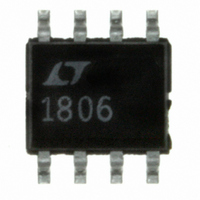
LT1806CS8 Linear Technology, LT1806CS8 Datasheet - Page 20

LT1806CS8
Manufacturer Part Number
LT1806CS8
Description
IC OPAMP R-R IN/OUT SNGL 8-SOIC
Manufacturer
Linear Technology
Datasheet
1.LT1806CS8PBF.pdf
(28 pages)
Specifications of LT1806CS8
Amplifier Type
General Purpose
Number Of Circuits
1
Output Type
Rail-to-Rail
Slew Rate
140 V/µs
Gain Bandwidth Product
325MHz
Current - Input Bias
5µA
Voltage - Input Offset
100µV
Current - Supply
11mA
Current - Output / Channel
85mA
Voltage - Supply, Single/dual (±)
2.5 V ~ 12.6 V, ±1.25 V ~ 6.3 V
Operating Temperature
0°C ~ 70°C
Mounting Type
Surface Mount
Package / Case
8-SOIC (3.9mm Width)
Lead Free Status / RoHS Status
Contains lead / RoHS non-compliant
-3db Bandwidth
-
Available stocks
Company
Part Number
Manufacturer
Quantity
Price
Part Number:
LT1806CS8
Manufacturer:
LINEAR/凌特
Quantity:
20 000
Company:
Part Number:
LT1806CS8#PBF
Manufacturer:
LT
Quantity:
1 469
Part Number:
LT1806CS8#PBF
Manufacturer:
LT
Quantity:
20 000
Part Number:
LT1806CS8#TRPBF
Manufacturer:
LINEAR/凌特
Quantity:
20 000
LT1806/LT1807
APPLICATIONS INFORMATION
The LT1806/LT1807’s input stages are also protected
against large differential input voltages of 1.4V or higher
by a pair of back-to-back diodes, D5/D8, that prevent
the emitter-base breakdown of the input transistors. The
current in these diodes should be limited to less than 10mA
when they are active. The worst-case differential input
voltage usually occurs when the input is driven while the
output is shorted to ground in a unity gain confi guration.
In addition, the amplifi er is protected against ESD strikes
up to 3kV on all pins by a pair of protection diodes, ESDD1
to ESDD6, on each pin that are connected to the power
supplies as shown in Figure 1.
Capacitive Load
The LT1806/LT1807 are optimized for high bandwidth and
low distortion applications. They can drive a capacitive
load of about 20pF in a unity-gain confi guration, and more
for higher gain. When driving a larger capacitive load, a
resistor of 10Ω to 50Ω should be connected between the
output and the capacitive load to avoid ringing or oscilla-
tion. The feedback should still be taken from the output so
that the resistor will isolate the capacitive load to ensure
stability. Graphs on capacitive loads indicate the transient
response of the amplifi er when driving the capacitive load
with a specifi ed series resistor.
20
Feedback Components
When feedback resistors are used to set up gain, care must
be taken to ensure that the pole formed by the feedback
resistors and the total capacitance at the inverting input
does not degrade stability. For instance, the LT1806/LT1807
in a noninverting gain of 2, set up with two 1k resistors
and a capacitance of 3pF (part plus PC board) will probably
ring in transient response. The pole is formed at 106MHz
that will reduce phase margin by 34 degrees when the
crossover frequency of the amplifi er is around 70MHz. A
capacitor of 3pF or higher connected across the feedback
resistor will eliminate any ringing or oscillation.
SHDN Pin
The LT1806 has a SHDN pin to reduce the supply current
to less than 0.9mA. When the SHDN pin is pulled low, it
will generate a signal to power down the device. If the pin
is left unconnected, an internal pull-up resistor of 40k will
keep the part fully operating as shown in Figure 1. The
output will be high impedance during shutdown, and the
turn-on and turn-off time is less than 100ns. Because
the input is protected by a pair of back-to-back diodes,
the input signal will feed through to the output during
shutdown mode if the amplitude of signal between the
inputs is larger than 1.4V.
18067fc


